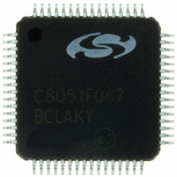
C8051F067-GQ Silicon Laboratories Inc, C8051F067-GQ Datasheet - Page 323

C8051F067-GQ
Manufacturer Part Number
C8051F067-GQ
Description
IC 8051 MCU 32K FLASH 64TQFP
Manufacturer
Silicon Laboratories Inc
Series
C8051F06xr
Specifications of C8051F067-GQ
Core Processor
8051
Core Size
8-Bit
Speed
25MHz
Connectivity
SMBus (2-Wire/I²C), SPI, UART/USART
Peripherals
Brown-out Detect/Reset, POR, PWM, WDT
Number Of I /o
24
Program Memory Size
32KB (32K x 8)
Program Memory Type
FLASH
Ram Size
4.25K x 8
Voltage - Supply (vcc/vdd)
2.7 V ~ 3.6 V
Data Converters
A/D 2x16b
Oscillator Type
Internal
Operating Temperature
-40°C ~ 85°C
Package / Case
64-TQFP, 64-VQFP
Processor Series
C8051F0x
Core
8051
Data Bus Width
8 bit
Data Ram Size
4.25 KB
Interface Type
I2C, SMBus, SPI, UART
Maximum Clock Frequency
25 MHz
Number Of Programmable I/os
24
Number Of Timers
5
Operating Supply Voltage
2.7 V to 3.6 V
Maximum Operating Temperature
+ 85 C
Mounting Style
SMD/SMT
3rd Party Development Tools
PK51, CA51, A51, ULINK2
Development Tools By Supplier
C8051F060DK
Minimum Operating Temperature
- 40 C
On-chip Adc
16 bit, 1 Channel
On-chip Dac
12 bit, 2 Channel
Lead Free Status / RoHS Status
Lead free / RoHS Compliant
Eeprom Size
-
Lead Free Status / Rohs Status
Details
Other names
336-1222
Available stocks
Company
Part Number
Manufacturer
Quantity
Price
Company:
Part Number:
C8051F067-GQ
Manufacturer:
AD
Quantity:
210
Company:
Part Number:
C8051F067-GQ
Manufacturer:
Silicon Laboratories Inc
Quantity:
10 000
Company:
Part Number:
C8051F067-GQR
Manufacturer:
Silicon Laboratories Inc
Quantity:
10 000
- Current page: 323 of 328
- Download datasheet (2Mb)
This register determines how the Flash interface logic will respond to reads and writes to the
FLASHDAT Register.
Bit7:
Bits6-4:
Bits3-0:
SFLE
Bit7
SFLE: Scratchpad Flash Memory Access Enable
When this bit is set, Flash reads and writes through the JTAG port are directed to the 128-
byte Scratchpad Flash sector. When SFLE is set to logic 1, Flash accesses out of the
address range 0x00-0x7F should not be attempted. Reads/Writes out of this range will yield
undefined results.
0: Flash access from JTAG directed to the Program/Data Flash sector.
1: Flash access from JTAG directed to the Scratchpad sector.
WRMD2-0: Write Mode Select Bits.
The Write Mode Select Bits control how the interface logic responds to writes to the FLASH-
DAT Register per the following values:
000:
ignored.
001:
FLASHADR register. FLASHADR is incremented by one when complete.
010:
containing the address in FLASHADR. The data written must be 0xA5 for the erase to occur.
FLASHADR is not affected. If FLASHADR = 0x7BFE - 0x7BFF, the entire user space will be
erased (i.e. entire Flash memory except for Reserved area 0x7C00 - 0x7FFF).
(All other values for WRMD2-0 are reserved.)
RDMD3-0: Read Mode Select Bits.
The Read Mode Select Bits control how the interface logic responds to reads to the FLASH-
DAT Register per the following values:
0000:
ignored.
0001:
if no operation is currently active. This mode is used for block reads.
0010:
operation is active and any data from a previous read has already been read from FLASH-
DAT. This mode allows single bytes to be read (or the last byte of a block) without initiating
an extra read.
(All other values for RDMD3-0 are reserved.)
WRMD2
Bit6
A FLASHDAT write replaces the data in the FLASHDAT register, but is otherwise
A FLASHDAT write initiates a write of FLASHDAT into the memory address by the
A FLASHDAT write initiates an erasure (sets all bytes to 0xFF) of the Flash page
A FLASHDAT read provides the data in the FLASHDAT register, but is otherwise
A FLASHDAT read initiates a read of the byte addressed by the FLASHADR register
A FLASHDAT read initiates a read of the byte addressed by FLASHADR only if no
Figure 26.3. FLASHCON: JTAG Flash Control Register
WRMD1
Bit5
WRMD0
Bit4
Rev. 1.2
RDMD3
Bit3
C8051F060/1/2/3/4/5/6/7
RDMD2
Bit2
RDMD1
Bit1
RDMD0
Bit0
Reset Value
00000000
323
Related parts for C8051F067-GQ
Image
Part Number
Description
Manufacturer
Datasheet
Request
R
Part Number:
Description:
SMD/C°/SINGLE-ENDED OUTPUT SILICON OSCILLATOR
Manufacturer:
Silicon Laboratories Inc
Part Number:
Description:
Manufacturer:
Silicon Laboratories Inc
Datasheet:
Part Number:
Description:
N/A N/A/SI4010 AES KEYFOB DEMO WITH LCD RX
Manufacturer:
Silicon Laboratories Inc
Datasheet:
Part Number:
Description:
N/A N/A/SI4010 SIMPLIFIED KEY FOB DEMO WITH LED RX
Manufacturer:
Silicon Laboratories Inc
Datasheet:
Part Number:
Description:
N/A/-40 TO 85 OC/EZLINK MODULE; F930/4432 HIGH BAND (REV E/B1)
Manufacturer:
Silicon Laboratories Inc
Part Number:
Description:
EZLink Module; F930/4432 Low Band (rev e/B1)
Manufacturer:
Silicon Laboratories Inc
Part Number:
Description:
I°/4460 10 DBM RADIO TEST CARD 434 MHZ
Manufacturer:
Silicon Laboratories Inc
Part Number:
Description:
I°/4461 14 DBM RADIO TEST CARD 868 MHZ
Manufacturer:
Silicon Laboratories Inc
Part Number:
Description:
I°/4463 20 DBM RFSWITCH RADIO TEST CARD 460 MHZ
Manufacturer:
Silicon Laboratories Inc
Part Number:
Description:
I°/4463 20 DBM RADIO TEST CARD 868 MHZ
Manufacturer:
Silicon Laboratories Inc
Part Number:
Description:
I°/4463 27 DBM RADIO TEST CARD 868 MHZ
Manufacturer:
Silicon Laboratories Inc
Part Number:
Description:
I°/4463 SKYWORKS 30 DBM RADIO TEST CARD 915 MHZ
Manufacturer:
Silicon Laboratories Inc
Part Number:
Description:
N/A N/A/-40 TO 85 OC/4463 RFMD 30 DBM RADIO TEST CARD 915 MHZ
Manufacturer:
Silicon Laboratories Inc
Part Number:
Description:
I°/4463 20 DBM RADIO TEST CARD 169 MHZ
Manufacturer:
Silicon Laboratories Inc


