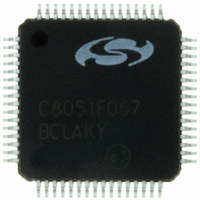
C8051F067-GQ Silicon Laboratories Inc, C8051F067-GQ Datasheet - Page 87

C8051F067-GQ
Manufacturer Part Number
C8051F067-GQ
Description
IC 8051 MCU 32K FLASH 64TQFP
Manufacturer
Silicon Laboratories Inc
Series
C8051F06xr
Specifications of C8051F067-GQ
Core Processor
8051
Core Size
8-Bit
Speed
25MHz
Connectivity
SMBus (2-Wire/I²C), SPI, UART/USART
Peripherals
Brown-out Detect/Reset, POR, PWM, WDT
Number Of I /o
24
Program Memory Size
32KB (32K x 8)
Program Memory Type
FLASH
Ram Size
4.25K x 8
Voltage - Supply (vcc/vdd)
2.7 V ~ 3.6 V
Data Converters
A/D 2x16b
Oscillator Type
Internal
Operating Temperature
-40°C ~ 85°C
Package / Case
64-TQFP, 64-VQFP
Processor Series
C8051F0x
Core
8051
Data Bus Width
8 bit
Data Ram Size
4.25 KB
Interface Type
I2C, SMBus, SPI, UART
Maximum Clock Frequency
25 MHz
Number Of Programmable I/os
24
Number Of Timers
5
Operating Supply Voltage
2.7 V to 3.6 V
Maximum Operating Temperature
+ 85 C
Mounting Style
SMD/SMT
3rd Party Development Tools
PK51, CA51, A51, ULINK2
Development Tools By Supplier
C8051F060DK
Minimum Operating Temperature
- 40 C
On-chip Adc
16 bit, 1 Channel
On-chip Dac
12 bit, 2 Channel
Lead Free Status / RoHS Status
Lead free / RoHS Compliant
Eeprom Size
-
Lead Free Status / Rohs Status
Details
Other names
336-1222
Available stocks
Company
Part Number
Manufacturer
Quantity
Price
Company:
Part Number:
C8051F067-GQ
Manufacturer:
AD
Quantity:
210
Company:
Part Number:
C8051F067-GQ
Manufacturer:
Silicon Laboratories Inc
Quantity:
10 000
Company:
Part Number:
C8051F067-GQR
Manufacturer:
Silicon Laboratories Inc
Quantity:
10 000
- Current page: 87 of 328
- Download datasheet (2Mb)
7.
The ADC2 subsystem for the C8051F060/1/2/3 consists of an analog multiplexer (referred to as AMUX2),
and a 200 ksps, 10-bit successive-approximation-register ADC with integrated track-and-hold and pro-
grammable window detector (see block diagram in Figure 7.1). The AMUX2, data conversion modes, and
window detector can all be configured from within software via the Special Function Registers shown in
Figure 7.1. ADC2 operates in both Single-ended and Differential modes, and may be configured to mea-
sure any of the pins on Port 1, or the Temperature Sensor output. The ADC2 subsystem is enabled only
when the AD2EN bit in the ADC2 Control register (ADC2CN) is set to logic 1. The ADC2 subsystem is in
low power shutdown when this bit is logic 0.
AIN2.0
AIN2.1
AIN2.2
AIN2.3
AIN2.4
AIN2.5
AIN2.6
AIN2.7
10-Bit ADC (ADC2, C8051F060/1/2/3)
SENSOR
AGND
TEMP
AMX2CF
ADC2GTH
AMUX
(SE or
9-to-1
DIFF)
AMX2SL
Figure 7.1. ADC2 Functional Block Diagram
ADC2GTL
ADC2CF
ADC2LTH
Rev. 1.2
AD2EN
C8051F060/1/2/3/4/5/6/7
ADC
10-Bit
AV+
SAR
ADC2CN
ADC2LTL
Start Conversion
10
20
Comb.
00
01
10
11
10
Logic
AD2BUSY (W)
Timer 3 Overflow
CNVSTR2
Timer 2 Overflow
AD2WINT
87
Related parts for C8051F067-GQ
Image
Part Number
Description
Manufacturer
Datasheet
Request
R
Part Number:
Description:
SMD/C°/SINGLE-ENDED OUTPUT SILICON OSCILLATOR
Manufacturer:
Silicon Laboratories Inc
Part Number:
Description:
Manufacturer:
Silicon Laboratories Inc
Datasheet:
Part Number:
Description:
N/A N/A/SI4010 AES KEYFOB DEMO WITH LCD RX
Manufacturer:
Silicon Laboratories Inc
Datasheet:
Part Number:
Description:
N/A N/A/SI4010 SIMPLIFIED KEY FOB DEMO WITH LED RX
Manufacturer:
Silicon Laboratories Inc
Datasheet:
Part Number:
Description:
N/A/-40 TO 85 OC/EZLINK MODULE; F930/4432 HIGH BAND (REV E/B1)
Manufacturer:
Silicon Laboratories Inc
Part Number:
Description:
EZLink Module; F930/4432 Low Band (rev e/B1)
Manufacturer:
Silicon Laboratories Inc
Part Number:
Description:
I°/4460 10 DBM RADIO TEST CARD 434 MHZ
Manufacturer:
Silicon Laboratories Inc
Part Number:
Description:
I°/4461 14 DBM RADIO TEST CARD 868 MHZ
Manufacturer:
Silicon Laboratories Inc
Part Number:
Description:
I°/4463 20 DBM RFSWITCH RADIO TEST CARD 460 MHZ
Manufacturer:
Silicon Laboratories Inc
Part Number:
Description:
I°/4463 20 DBM RADIO TEST CARD 868 MHZ
Manufacturer:
Silicon Laboratories Inc
Part Number:
Description:
I°/4463 27 DBM RADIO TEST CARD 868 MHZ
Manufacturer:
Silicon Laboratories Inc
Part Number:
Description:
I°/4463 SKYWORKS 30 DBM RADIO TEST CARD 915 MHZ
Manufacturer:
Silicon Laboratories Inc
Part Number:
Description:
N/A N/A/-40 TO 85 OC/4463 RFMD 30 DBM RADIO TEST CARD 915 MHZ
Manufacturer:
Silicon Laboratories Inc
Part Number:
Description:
I°/4463 20 DBM RADIO TEST CARD 169 MHZ
Manufacturer:
Silicon Laboratories Inc


