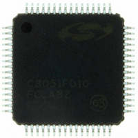
C8051F010-GQ Silicon Laboratories Inc, C8051F010-GQ Datasheet - Page 107

C8051F010-GQ
Manufacturer Part Number
C8051F010-GQ
Description
IC 8051 MCU 32K FLASH 64TQFP
Manufacturer
Silicon Laboratories Inc
Series
C8051F01xr
Specifications of C8051F010-GQ
Core Processor
8051
Core Size
8-Bit
Speed
20MHz
Connectivity
SMBus (2-Wire/I²C), SPI, UART/USART
Peripherals
Brown-out Detect/Reset, POR, PWM, Temp Sensor, WDT
Number Of I /o
32
Program Memory Size
32KB (32K x 8)
Program Memory Type
FLASH
Ram Size
256 x 8
Voltage - Supply (vcc/vdd)
2.7 V ~ 3.6 V
Data Converters
A/D 8x10b; D/A 2x12b
Oscillator Type
Internal
Operating Temperature
-40°C ~ 85°C
Package / Case
64-TQFP, 64-VQFP
Processor Series
C8051F0x
Core
8051
Data Bus Width
8 bit
Data Ram Size
256 B
Interface Type
I2C, SMBus, SPI, UART
Maximum Clock Frequency
20 MHz
Number Of Programmable I/os
32
Number Of Timers
4 bit
Operating Supply Voltage
2.7 V to 3.6 V
Maximum Operating Temperature
+ 85 C
Mounting Style
SMD/SMT
3rd Party Development Tools
PK51, CA51, A51, ULINK2
Development Tools By Supplier
C8051F005DK
Minimum Operating Temperature
- 40 C
On-chip Adc
10 bit, 8 Channel
On-chip Dac
12 bit, 2 Channel
Lead Free Status / RoHS Status
Lead free / RoHS Compliant
Eeprom Size
-
Lead Free Status / Rohs Status
Details
Other names
336-1191
Available stocks
Company
Part Number
Manufacturer
Quantity
Price
Company:
Part Number:
C8051F010-GQ
Manufacturer:
Silicon Laboratories Inc
Quantity:
10 000
107
C8051F000/1/2/5/6/7
C8051F010/1/2/5/6/7
SYSCKE
Bit7:
Bit6:
Bit5:
Bit4:
Bit3:
Bit2:
Bit1:
Bit0:
R/W
Bit7
0: SYSCLK unavailable at Port pin.
1: SYSCLK output routed to Port Pin.
0: T2EX unavailable at Port pin.
1: T2EX routed to Port Pin.
T2E: T2 Enable Bit
0: T2 unavailable at Port pin.
1: T2 routed to Port Pin.
0: /INT1 unavailable at Port pin.
1: /INT1 routed to Port Pin.
T1E: T1 Enable Bit
0: T1 unavailable at Port pin.
1: T1 routed to Port Pin.
0: /INT0 unavailable at Port pin.
1: /INT0 routed to Port Pin.
T0E: T0 Enable Bit
0: T0 unavailable at Port pin.
1: T0 routed to Port Pin.
0: CP1 unavailable at Port pin.
1: CP1 routed to Port Pin.
SYSCKE: SYSCLK Output Enable Bit
T2EXE: T2EX Enable Bit
INT1E: /INT1 Enable Bit
INT0E: /INT0 Enable Bit
CP1OEN: Comparator 1 Output Enable Bit
T2EXE
R/W
Bit6
Figure 15.4. XBR1: Port I/O CrossBar Register 1
R/W
T2E
Bit5
INT1E
R/W
Bit4
Rev. 1.7
T1E
R/W
Bit3
INT0E
R/W
Bit2
R/W
T0E
Bit1
CP1OEN
R/W
Bit0
SFR Address:
Reset Value
00000000
0xE2


