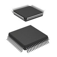
DF36034HJV Renesas Electronics America, DF36034HJV Datasheet - Page 234

DF36034HJV
Manufacturer Part Number
DF36034HJV
Description
MCU 3/5V 32K J-TEMP PB-FREE 64-Q
Manufacturer
Renesas Electronics America
Series
H8® H8/300H Tinyr
Specifications of DF36034HJV
Core Processor
H8/300H
Core Size
16-Bit
Speed
20MHz
Connectivity
CAN, SCI, SSU
Peripherals
PWM, WDT
Number Of I /o
45
Program Memory Size
32KB (32K x 8)
Program Memory Type
FLASH
Ram Size
2K x 8
Voltage - Supply (vcc/vdd)
3 V ~ 5.5 V
Data Converters
A/D 8x10b
Oscillator Type
Internal
Operating Temperature
-40°C ~ 85°C
Package / Case
64-QFP
For Use With
R0K436079S000BE - KIT DEV FOR H8/36079 W/COMPILER
Lead Free Status / RoHS Status
Lead free / RoHS Compliant
Eeprom Size
-
- Current page: 234 of 594
- Download datasheet (4Mb)
Section 12 Timer Z
12.4.5
In PWM mode, PWM waveforms are output from the FTIOB, FTIOC, and FTIOD output pins
with GRA as a cycle register and GRB, GRC, and GRD as duty registers. The initial output level
of the corresponding pin depends on the setting values of TOCR and POCR. Table 12.3 shows an
example of the initial output level of the FTIOB0 pin.
The output level is determined by the POLB to POLD bits corresponding to POCR. When POLB
is 0, the FTIOB output pin is set to 0 by compare match B and set to 1 by compare match A. When
POLB is 1, the FTIOB output pin is set to 1 by compare match B and cleared to 0 by compare
match A. In PWM mode, maximum 6-phase PWM outputs are possible.
Figure 12.21 shows an example of the PWM mode setting procedure.
Table 12.3 Initial Output Level of FTIOB0 Pin
TOB0
0
0
1
1
Rev. 4.00 Mar. 15, 2006 Page 200 of 556
REJ09B0026-0400
PWM Mode
POLB
0
1
0
1
Initial Output Level
1
0
0
1
Related parts for DF36034HJV
Image
Part Number
Description
Manufacturer
Datasheet
Request
R

Part Number:
Description:
Headers & Wire Housings 20P PLUG METAL COVER
Manufacturer:
Hirose Electric Co Ltd

Part Number:
Description:
Headers & Wire Housings 25P PLUG METAL COVER
Manufacturer:
Hirose Electric Co Ltd

Part Number:
Description:
Headers & Wire Housings 15P PLUG METAL COVER
Manufacturer:
Hirose Electric Co Ltd

Part Number:
Description:
0.4 Mm Pitch, 1.5 Mm Mated Height, Board-to-fine Coaxial Cable Connectors
Manufacturer:
Hirose Electric
Datasheet:

Part Number:
Description:
CONN RECEPT 40POS 0.4MM SMD GOLD
Manufacturer:
Hirose Electric Co Ltd
Datasheet:

Part Number:
Description:
KIT STARTER FOR M16C/29
Manufacturer:
Renesas Electronics America
Datasheet:

Part Number:
Description:
KIT STARTER FOR R8C/2D
Manufacturer:
Renesas Electronics America
Datasheet:

Part Number:
Description:
R0K33062P STARTER KIT
Manufacturer:
Renesas Electronics America
Datasheet:

Part Number:
Description:
KIT STARTER FOR R8C/23 E8A
Manufacturer:
Renesas Electronics America
Datasheet:

Part Number:
Description:
KIT STARTER FOR R8C/25
Manufacturer:
Renesas Electronics America
Datasheet:

Part Number:
Description:
KIT STARTER H8S2456 SHARPE DSPLY
Manufacturer:
Renesas Electronics America
Datasheet:

Part Number:
Description:
KIT STARTER FOR R8C38C
Manufacturer:
Renesas Electronics America
Datasheet:

Part Number:
Description:
KIT STARTER FOR R8C35C
Manufacturer:
Renesas Electronics America
Datasheet:

Part Number:
Description:
KIT STARTER FOR R8CL3AC+LCD APPS
Manufacturer:
Renesas Electronics America
Datasheet:

Part Number:
Description:
KIT STARTER FOR RX610
Manufacturer:
Renesas Electronics America
Datasheet:


