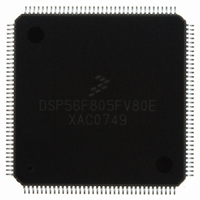
DSP56F805FV80E Freescale Semiconductor, DSP56F805FV80E Datasheet - Page 3

DSP56F805FV80E
Manufacturer Part Number
DSP56F805FV80E
Description
IC DSP 80MHZ 31.5K FLASH 144LQFP
Manufacturer
Freescale Semiconductor
Series
56F8xxr
Datasheet
1.DSP56F805FV80E.pdf
(56 pages)
Specifications of DSP56F805FV80E
Core Processor
56800
Core Size
16-Bit
Speed
80MHz
Connectivity
CAN, EBI/EMI, SCI, SPI
Peripherals
POR, PWM, WDT
Number Of I /o
32
Program Memory Size
71KB (35.5K x 16)
Program Memory Type
FLASH
Ram Size
2.5K x 16
Voltage - Supply (vcc/vdd)
3 V ~ 3.6 V
Data Converters
A/D 8x12b
Oscillator Type
External
Operating Temperature
-40°C ~ 85°C
Package / Case
144-LQFP
Product
DSPs
Data Bus Width
16 bit
Processor Series
DSP56F8xx
Core
56800
Numeric And Arithmetic Format
Fixed-Point
Instruction Set Architecture
MAC
Device Million Instructions Per Second
40 MIPs
Maximum Clock Frequency
80 MHz
Number Of Programmable I/os
32
Data Ram Size
4 KB
Operating Supply Voltage
3 V to 3.6 V
Maximum Operating Temperature
+ 85 C
Mounting Style
SMD/SMT
Development Tools By Supplier
PBMCUSLK, DSP56F800DEMO-E
Interface Type
SCI, SPI
Minimum Operating Temperature
- 40 C
On-chip Adc
12 bit, 4 Channel
Lead Free Status / RoHS Status
Lead free / RoHS Compliant
Eeprom Size
-
Lead Free Status / Rohs Status
Lead free / RoHS Compliant
Available stocks
Company
Part Number
Manufacturer
Quantity
Price
Company:
Part Number:
DSP56F805FV80E
Manufacturer:
ST
Quantity:
7 000
Company:
Part Number:
DSP56F805FV80E
Manufacturer:
QFP
Quantity:
885
Company:
Part Number:
DSP56F805FV80E
Manufacturer:
Freescale Semiconductor
Quantity:
10 000
Part Number:
DSP56F805FV80E
Manufacturer:
NXP/恩智浦
Quantity:
20 000
Freescale Semiconductor
56F805 General Description
*
•
•
•
•
•
•
•
•
•
•
includes TCS pin which is reserved for factory use and is tied to VSS
3
4
3
4
4
4
2
4
2
2
2
4
14
4
4
Up to 40 MIPS at 80MHz core frequency
DSP and MCU functionality in a unified,
C-efficient architecture
Hardware DO and REP loops
MCU-friendly instruction set supports both DSP
and controller functions: MAC, bit manipulation
unit, 14 addressing modes
31.5K × 16-bit words (64KB) Program Flash
512 × 16-bit words (1KB) Program RAM
4K × 16-bit words (8KB) Data Flash
2K × 16-bit words (4KB) Data RAM
2K × 16-bit words (4KB) Boot Flash
Up to 64K × 16-bit words (128KB) each of external
Program and Data memory
6
6
Current Sense Inputs
Fault Inputs
Current Sense Inputs
Fault Inputs
A/D1
A/D2
VREF
Quad Timer C
PWM Outputs
PWM Outputs
Quad Timer A
Quad Timer D
Quad B Timer
CAN 2.0A/B
Quadrature
Decoder 0/
Quadrature
Dedicated
Decoder 1/
/ Alt Func
GPIO
GPIO
GPIO
GPIO
SCI0
SCI1
SPI
or
or
or
ADC
tion-Specific
Peripherals
Program Memory
32252 x 16 Flash
2048 x 16 SRAM
Memory &
512 x 16 SRAM
2048 x 16 Flash
4096 x 16 Flash
Applica-
Data Memory
Boot Flash
Watchdog
Controller
PWMA
PWMB
Interrupt
COP/
RSTO
RESET
Hardware Looping Unit
•
MODULE CONTROLS
ADDRESS BUS [8:0]
Program Controller
DATA BUS [15:0]
56F805 Technical Data, Rev. 16
56F805 Block Diagram
•
COP RESET
IRQA
•
and
IRQB
EXTBOOT
CGDB
XAB1
XAB2
XDB2
PDB
PAB
INTERRUPT
CONTROLS
6
JTAG/
OnCE
Port
Generation
•
Address
Unit
•
IPBus Bridge
16
VPP
•
•
•
•
•
•
•
•
•
•
•
(IPBB)
•
CONTROLS
VCAPC V
2
IPBB
Two 6-channel PWM Modules
Two 4-channel, 12-bit ADCs
Two Quadrature Decoders
CAN 2.0 B Module
Two Serial Communication Interfaces (SCIs)
Serial Peripheral Interface (SPI)
Up to four General Purpose Quad Timers
JTAG/OnCE
14 Dedicated and 18 Shared GPIO lines
144-pin LQFP Package
Three 16-bit Input Registers
16 x 16 + 36 → 36-Bit MAC
Two 36-bit Accumulators
8
16
Digital Reg
•
DD
Data ALU
8*
16-Bit
56800
V
Low Voltage
Core
Supervisor
SS
Interface
TM
External
Bus
Unit
V
port for debugging
DDA
Analog Reg
Manipulation
Address Bus
Clock Gen
V
Data Bus
External
External
Control
SSA
Switch
Switch
PLL
Bus
Unit
Bit
6
16
10
A[00:05]
A[06:15] or
GPIO-E2:E3 &
GPIO-A0:A7
D[00:15]
PS Select
DS Select
WR Enable
RD Enable
EXTAL
CLKO
XTAL
3


