DF2367VF33V Renesas Electronics America, DF2367VF33V Datasheet - Page 327
DF2367VF33V
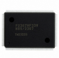
Manufacturer Part Number
DF2367VF33V
Description
IC H8S/2367 MCU FLASH 128QFP
Manufacturer
Renesas Electronics America
Series
H8® H8S/2300r
Datasheets
1.HEWH8E10A.pdf
(19 pages)
2.D12312SVTE25V.pdf
(341 pages)
3.DF2368VTE34V.pdf
(1044 pages)
Specifications of DF2367VF33V
Core Processor
H8S/2000
Core Size
16-Bit
Speed
33MHz
Connectivity
I²C, IrDA, SCI, SmartCard
Peripherals
DMA, POR, PWM, WDT
Number Of I /o
84
Program Memory Size
384KB (384K x 8)
Program Memory Type
FLASH
Ram Size
24K x 8
Voltage - Supply (vcc/vdd)
3 V ~ 3.6 V
Data Converters
A/D 10x10b, D/A 2x8b
Oscillator Type
Internal
Operating Temperature
-20°C ~ 75°C
Package / Case
128-QFP
For Use With
YR0K42378FC000BA - KIT EVAL FOR H8S/2378HS0005KCU11H - EMULATOR E10A-USB H8S(X),SH2(A)
Lead Free Status / RoHS Status
Lead free / RoHS Compliant
Eeprom Size
-
Available stocks
Company
Part Number
Manufacturer
Quantity
Price
Company:

Part Number:
DF2367VF33V
Manufacturer:
Renesas Electronics America
Quantity:
135
Company:
Part Number:
DF2367VF33V
Manufacturer:
Renesas Electronics America
Quantity:
10 000


7.5.8
An example of the basic DMAC bus cycle timing is shown in figure 7.17. In this example, word-
size transfer is performed from 16-bit, 2-state access space to 8-bit, 3-state access space. When
the bus is transferred from the CPU to the DMAC, a source address read and destination address
write are performed. The bus is not released in response to another bus request, etc., between
these read and write operations. As like CPU cycles, DMA cycles conform to the bus controller
settings.
The address is not output to the external address bus in an access to on-chip memory or an internal
I/O register.
7.5.9
Short Address Mode: Figure 7.18 shows a transfer example in which TEND output is enabled
and byte-size short address mode transfer (sequential/idle/repeat mode) is performed from external
8-bit, 2-state access space to internal I/O space.
Basic Bus Cycles
DMA Transfer (Dual Address Mode) Bus Cycles
Address bus
CPU cycle
Figure 7.17 Example of DMA Transfer Bus Timing
T
1
address
Source
T
2
DMAC cycle (1-word transfer)
T
1
T
Destination address
2
T
3
T
Rev.6.00 Mar. 18, 2009 Page 267 of 980
1
T
2
Section 7 DMA Controller (DMAC)
T
3
CPU cycle
REJ09B0050-0600
Related parts for DF2367VF33V
Image
Part Number
Description
Manufacturer
Datasheet
Request
R

Part Number:
Description:
CONN PLUG 12POS DUAL 0.5MM SMD
Manufacturer:
Hirose Electric Co Ltd
Datasheet:
Part Number:
Description:
CONN PLUG 18POS DUAL 0.5MM SMD
Manufacturer:
Hirose Electric Co Ltd
Datasheet:
Part Number:
Description:
CONN PLUG 14POS DUAL 0.5MM SMD
Manufacturer:
Hirose Electric Co Ltd
Datasheet:
Part Number:
Description:
CONN RECEPT 20POS DUAL 0.5MM SMD
Manufacturer:
Hirose Electric Co Ltd
Datasheet:
Part Number:
Description:
CONN PLUG 16POS DUAL 0.5MM SMD
Manufacturer:
Hirose Electric Co Ltd
Datasheet:
Part Number:
Description:
CONN RECEPT 16POS DUAL 0.5MM SMD
Manufacturer:
Hirose Electric Co Ltd
Datasheet:
Part Number:
Description:
CONN PLUG 20POS DUAL 0.5MM SMD
Manufacturer:
Hirose Electric Co Ltd
Datasheet:
Part Number:
Description:
CONN PLUG 30POS DUAL 0.5MM SMD
Manufacturer:
Hirose Electric Co Ltd
Datasheet:
Part Number:
Description:
CONN RECEPT 30POS DUAL 0.5MM SMD
Manufacturer:
Hirose Electric Co Ltd
Datasheet:
Part Number:
Description:
CONN PLUG 40POS DUAL 0.5MM SMD
Manufacturer:
Hirose Electric Co Ltd
Datasheet:

Part Number:
Description:
KIT STARTER FOR M16C/29
Manufacturer:
Renesas Electronics America
Datasheet:

Part Number:
Description:
KIT STARTER FOR R8C/2D
Manufacturer:
Renesas Electronics America
Datasheet:

Part Number:
Description:
R0K33062P STARTER KIT
Manufacturer:
Renesas Electronics America
Datasheet:

Part Number:
Description:
KIT STARTER FOR R8C/23 E8A
Manufacturer:
Renesas Electronics America
Datasheet:

Part Number:
Description:
KIT STARTER FOR R8C/25
Manufacturer:
Renesas Electronics America
Datasheet: