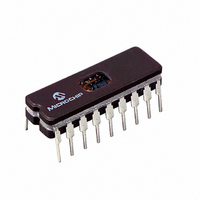
PIC16C554/JW Microchip Technology, PIC16C554/JW Datasheet - Page 31

PIC16C554/JW
Manufacturer Part Number
PIC16C554/JW
Description
IC MCU EPROM 512X14 18CDIP
Manufacturer
Microchip Technology
Series
PIC® 16Cr
Specifications of PIC16C554/JW
Core Processor
PIC
Core Size
8-Bit
Speed
20MHz
Peripherals
POR, WDT
Number Of I /o
13
Program Memory Size
896B (512 x 14)
Program Memory Type
EPROM, UV
Ram Size
80 x 8
Voltage - Supply (vcc/vdd)
2.5 V ~ 5.5 V
Oscillator Type
External
Operating Temperature
0°C ~ 70°C
Package / Case
18-CDIP (0.300", 7.62mm) Window
Lead Free Status / RoHS Status
Contains lead / RoHS non-compliant
Eeprom Size
-
Data Converters
-
Connectivity
-
EXAMPLE 5-1:
FIGURE 5-6:
2002 Microchip Technology Inc.
; Initial PORT settings: PORTB<7:4> Inputs
;
;
; PORTB<7:6> have external pull-up and are
; not connected to other circuitry
;
;
;
;
Note 1: This example shows write to PORTB followed by a read from PORTB.
BCF PORTB, 7
BCF PORTB, 6
BSF STATUS, RP0 ;
BCF TRISB, 7
BCF TRISB, 6
Instruction
2: Data setup time = (0.25 T
RB <7:0>
fetched
output valid. Therefore, at higher clock frequencies, a write followed by a read may be problematic.
PC
READ-MODIFY-WRITE
INSTRUCTIONS ON AN
I/O PORT
SUCCESSIVE I/O OPERATION
Q1
MOVWF PORTB
; 01pp pppp
; 10pp pppp
; 10pp pppp
; 10pp pppp
PORT latch PORT pins
---------- ---------
Q2
Write to
PORTB
PORTB<3:0> Outputs
PC
Q3
CY
Q4
- T
11pp pppp
11pp pppp
11pp pppp
10pp pppp
PD
) where T
Q1
MOVF PORTB, W
Read PORTB
MOVWF
Preliminary
Execute
PORTB
Q2
PC + 1
CY
T
Q3
= instruction cycle and T
PD
Q4
5.4.2
The actual write to an I/O port happens at the end of an
instruction cycle, whereas for reading, the data must be
valid at the beginning of the instruction cycle, as shown
in Figure 5-6. Therefore, care must be exercised if a
write followed by a read operation is carried out on the
same I/O port. The sequence of instructions should be
such to allow the pin voltage to stabilize (load
dependent) before the next instruction which causes
that file to be read into the CPU is executed. Otherwise,
the previous state of that pin may be read into the CPU
rather than the new state. When in doubt, it is better to
separate these instructions with an NOP or another
instruction not accessing this I/O port.
Q1
Port pin
sampled here
Q2
PORTB, W
PC + 2
Execute
NOP
MOVF
SUCCESSIVE OPERATIONS ON I/O
PORTS
Q3
PD
= propagation delay of Q1 cycle to
Q4
Q1
PIC16C55X
Execute
Q2
PC + 3
NOP
NOP
Q3
DS40143D-page 29
Q4


