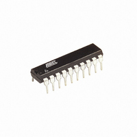
ATTINY2313-20PJ Atmel, ATTINY2313-20PJ Datasheet - Page 51

ATTINY2313-20PJ
Manufacturer Part Number
ATTINY2313-20PJ
Description
IC MCU AVR 2K FLASH 20DIP
Manufacturer
Atmel
Series
AVR® ATtinyr
Specifications of ATTINY2313-20PJ
Core Processor
AVR
Core Size
8-Bit
Speed
20MHz
Connectivity
SPI, UART/USART
Peripherals
Brown-out Detect/Reset, POR, PWM, WDT
Number Of I /o
18
Program Memory Size
2KB (1K x 16)
Program Memory Type
FLASH
Eeprom Size
128 x 8
Ram Size
128 x 8
Voltage - Supply (vcc/vdd)
2.7 V ~ 5.5 V
Oscillator Type
Internal
Operating Temperature
-40°C ~ 85°C
Package / Case
20-DIP (0.300", 7.62mm)
Lead Free Status / RoHS Status
Lead free / RoHS Compliant
Data Converters
-
Other names
ATTINY2313-24PJ
ATTINY2313-24PJ
ATTINY2313-24PJ
- Current page: 51 of 226
- Download datasheet (4Mb)
Alternate Port
Functions
2543L–AVR–08/10
Most port pins have alternate functions in addition to being general digital I/Os.
how the port pin control signals from the simplified
functions. The overriding signals may not be present in all port pins, but the figure serves as a
generic description applicable to all port pins in the AVR microcontroller family.
Figure 25. Alternate Port Functions
Note:
Table 23
ure 25
the modules having the alternate function.
PTOExn:
PUOExn:
PUOVxn:
DDOExn:
DDOVxn:
PVOExn:
PVOVxn:
DIEOExn: Pxn DIGITAL INPUT-ENABLE OVERRIDE ENABLE
DIEOVxn: Pxn DIGITAL INPUT-ENABLE OVERRIDE VALUE
SLEEP:
Pxn
are not shown in the succeeding tables. The overriding signals are generated internally in
1. WRx, WPx, WDx, RRx, RPx, and RDx are common to all pins within the same port. clk
summarizes the function of the overriding signals. The pin and port indexes from
SLEEP, and PUD are common to all ports. All other signals are unique for each pin.
Pxn, PORT TOGGLE OVERRIDE ENABLE
Pxn PULL-UP OVERRIDE ENABLE
Pxn PULL-UP OVERRIDE VALUE
Pxn DATA DIRECTION OVERRIDE ENABLE
Pxn DATA DIRECTION OVERRIDE VALUE
Pxn PORT VALUE OVERRIDE ENABLE
Pxn PORT VALUE OVERRIDE VALUE
SLEEP CONTROL
1
0
1
0
1
0
1
0
(1)
PUOExn
PUOVxn
DDOExn
DDOVxn
PVOExn
PVOVxn
DIEOExn
DIEOVxn
SLEEP
PUD:
WDx:
RDx:
RRx:
WRx:
RPx:
WPx:
clk
DIxn:
AIOxn:
SYNCHRONIZER
D
L
I/O
SET
CLR
:
Q
Q
Figure 22
PULLUP DISABLE
WRITE DDRx
READ DDRx
READ PORTx REGISTER
WRITE PORTx
READ PORTx PIN
I/O CLOCK
DIGITAL INPUT PIN n ON PORTx
ANALOG INPUT/OUTPUT PIN n ON PORTx
D
WRITE PINx
PINxn
CLR
Q
Q
RESET
RESET
PORTxn
Q
Q
Q
Q
DDxn
CLR
CLR
D
D
can be overridden by alternate
1
0
clk
PUD
WDx
RDx
RRx
DIxn
AIOxn
RPx
I/O
WRx
PTOExn
WPx
Figure 25
shows
Fig-
I/O
51
,
Related parts for ATTINY2313-20PJ
Image
Part Number
Description
Manufacturer
Datasheet
Request
R

Part Number:
Description:
IC, MCU, 8BIT, 2K FLASH, 20SOIC
Manufacturer:
Atmel
Datasheet:

Part Number:
Description:
IC, MCU, 8BIT, 2K FLASH, 20PDIP
Manufacturer:
Atmel
Datasheet:

Part Number:
Description:
IC, MCU, 8BIT, 8K FLASH, 20PDIP
Manufacturer:
Atmel
Datasheet:

Part Number:
Description:
IC, MCU, 8BIT, 8K FLASH, 20SOIC
Manufacturer:
Atmel
Datasheet:

Part Number:
Description:
DEV KIT FOR AVR/AVR32
Manufacturer:
Atmel
Datasheet:

Part Number:
Description:
INTERVAL AND WIPE/WASH WIPER CONTROL IC WITH DELAY
Manufacturer:
ATMEL Corporation
Datasheet:

Part Number:
Description:
Low-Voltage Voice-Switched IC for Hands-Free Operation
Manufacturer:
ATMEL Corporation
Datasheet:

Part Number:
Description:
MONOLITHIC INTEGRATED FEATUREPHONE CIRCUIT
Manufacturer:
ATMEL Corporation
Datasheet:

Part Number:
Description:
AM-FM Receiver IC U4255BM-M
Manufacturer:
ATMEL Corporation
Datasheet:

Part Number:
Description:
Monolithic Integrated Feature Phone Circuit
Manufacturer:
ATMEL Corporation
Datasheet:

Part Number:
Description:
Multistandard Video-IF and Quasi Parallel Sound Processing
Manufacturer:
ATMEL Corporation
Datasheet:

Part Number:
Description:
High-performance EE PLD
Manufacturer:
ATMEL Corporation
Datasheet:


