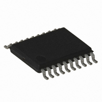
AT89LP2052-16XI Atmel, AT89LP2052-16XI Datasheet - Page 21

AT89LP2052-16XI
Manufacturer Part Number
AT89LP2052-16XI
Description
IC 8051 MCU FLASH 2K 20TSSOP
Manufacturer
Atmel
Series
89LPr
Datasheet
1.AT89LP2052-20PU.pdf
(94 pages)
Specifications of AT89LP2052-16XI
Core Processor
8051
Core Size
8-Bit
Speed
16MHz
Connectivity
SPI, UART/USART
Peripherals
Brown-out Detect/Reset, POR, PWM, WDT
Number Of I /o
15
Program Memory Size
2KB (2K x 8)
Program Memory Type
FLASH
Ram Size
256 x 8
Voltage - Supply (vcc/vdd)
2.4 V ~ 5.5 V
Oscillator Type
Internal
Operating Temperature
-40°C ~ 85°C
Package / Case
20-TSSOP
Lead Free Status / RoHS Status
Contains lead / RoHS non-compliant
Eeprom Size
-
Data Converters
-
Other names
AT89LP2052-20XI
AT89LP2052-20XI
AT89LP2052-20XI
15.2
3547J–MICRO–10/09
Input-only Mode
A second pull-up, called the “weak” pull-up, is turned on when the port register for the pin con-
tains a logic “1” and the pin itself is also at a logic “1” level. This pull-up provides the primary
source current for a quasi-bidirectional pin that is outputting a 1. If this pin is pulled low by an
external device, this weak pull-up turns off, and only the very weak pull-up remains on. In order
to pull the pin low under these conditions, the external device has to sink enough current to over-
power the weak pull-up and pull the port pin below its input threshold voltage.
The third pull-up is referred to as the “strong” pull-up. This pull-up is used to speed up low-to-
high transitions on a quasi-bidirectional port pin when the port register changes from a logic “0”
to a logic “1”. When this occurs, the strong pull-up turns on for one CPU clock, quickly pulling the
port pin high.
When in quasi-bidirectional mode the port pin will always output a “0” when corresponding bit in
the port register is also “0”. When the port register is “1” the pin may be used either as an input
or an output of “1”. The quasi-bidirectional port configuration is shown in
circuitry of P3.2 and P3.3 is not disabled during Power-down (see
Figure 15-1. Quasi-bidirectional Output
The input port configuration is shown in
input noise rejection.
Figure 15-2. Input Only
Figure 15-3. Input Only for P3.2 and P3.3
Register
From Port
Input
Input
Data
Data
PWD
1 Clock Delay
(D Flip-Flop)
Figure
Input
Data
15-2. It is a Schmitt-triggered input for improved
PWD
V
Strong
CC
AT89LP2052/LP4052
V
Weak
Very
CC
Figure
Port
Port
Pin
Pin
V
Weak
CC
15-3).
Figure
Port
Pin
15-1. The input
21


