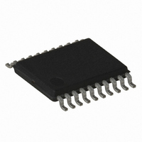
AT89LP2052-16XI Atmel, AT89LP2052-16XI Datasheet - Page 47

AT89LP2052-16XI
Manufacturer Part Number
AT89LP2052-16XI
Description
IC 8051 MCU FLASH 2K 20TSSOP
Manufacturer
Atmel
Series
89LPr
Datasheet
1.AT89LP2052-20PU.pdf
(94 pages)
Specifications of AT89LP2052-16XI
Core Processor
8051
Core Size
8-Bit
Speed
16MHz
Connectivity
SPI, UART/USART
Peripherals
Brown-out Detect/Reset, POR, PWM, WDT
Number Of I /o
15
Program Memory Size
2KB (2K x 8)
Program Memory Type
FLASH
Ram Size
256 x 8
Voltage - Supply (vcc/vdd)
2.4 V ~ 5.5 V
Oscillator Type
Internal
Operating Temperature
-40°C ~ 85°C
Package / Case
20-TSSOP
Lead Free Status / RoHS Status
Contains lead / RoHS non-compliant
Eeprom Size
-
Data Converters
-
Other names
AT89LP2052-20XI
AT89LP2052-20XI
AT89LP2052-20XI
- Current page: 47 of 94
- Download datasheet (2Mb)
19.3
3547J–MICRO–10/09
Serial Clock Generator
Figure 19-3. SPI Shift Register Diagram
The CPHA (Clock PHAse), CPOL (Clock POLarity), and SPR (Serial Peripheral clock Rate =
baud rate) bits in SPCR control the shape and rate of SCK. The two SPR bits provide four possi-
ble clock rates when the SPI is in master mode. In slave mode, the SPI will operate at the rate of
the incoming SCK as long as it does not exceed the maximum bit rate. There are also four pos-
sible combinations of SCK phase and polarity with respect to the serial data. CPHA and CPOL
determine which format is used for transmission. The SPI data transfer formats are shown in
Figures 19-4 and
CPOL, and SPR should be set up before the interface is enabled, and the master device should
be enabled before the slave device(s).
Transmit
Serial In
Byte
8
and 19-5. To prevent glitches on SCK from disrupting the interface, CPHA,
MUX
8
2:1
8
Parallel Master
Serial Master
(Write Buffer)
D
CLK
D
CLK
LATCH
LATCH
Q
Q
7
AT89LP2052/LP4052
MUX
2:1
8
Parallel Slave
Serial Slave
(Read Buffer)
D
CLK
D
CLK
LATCH
LATCH
Q
Q
8
Serial Out
Receive
Byte
47
Related parts for AT89LP2052-16XI
Image
Part Number
Description
Manufacturer
Datasheet
Request
R

Part Number:
Description:
DEV KIT FOR AVR/AVR32
Manufacturer:
Atmel
Datasheet:

Part Number:
Description:
INTERVAL AND WIPE/WASH WIPER CONTROL IC WITH DELAY
Manufacturer:
ATMEL Corporation
Datasheet:

Part Number:
Description:
Low-Voltage Voice-Switched IC for Hands-Free Operation
Manufacturer:
ATMEL Corporation
Datasheet:

Part Number:
Description:
MONOLITHIC INTEGRATED FEATUREPHONE CIRCUIT
Manufacturer:
ATMEL Corporation
Datasheet:

Part Number:
Description:
AM-FM Receiver IC U4255BM-M
Manufacturer:
ATMEL Corporation
Datasheet:

Part Number:
Description:
Monolithic Integrated Feature Phone Circuit
Manufacturer:
ATMEL Corporation
Datasheet:

Part Number:
Description:
Multistandard Video-IF and Quasi Parallel Sound Processing
Manufacturer:
ATMEL Corporation
Datasheet:

Part Number:
Description:
High-performance EE PLD
Manufacturer:
ATMEL Corporation
Datasheet:

Part Number:
Description:
8-bit Flash Microcontroller
Manufacturer:
ATMEL Corporation
Datasheet:

Part Number:
Description:
2-Wire Serial EEPROM
Manufacturer:
ATMEL Corporation
Datasheet:


