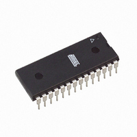
ATMEGA88PA-PU Atmel, ATMEGA88PA-PU Datasheet - Page 151

ATMEGA88PA-PU
Manufacturer Part Number
ATMEGA88PA-PU
Description
MCU AVR 8K ISP FLASH MEM 28-DIP
Manufacturer
Atmel
Series
AVR® ATmegar
Datasheets
1.ATMEGA48A-PU.pdf
(566 pages)
2.ATMEGA48A-PU.pdf
(33 pages)
3.ATMEGA48PA-MMH.pdf
(26 pages)
Specifications of ATMEGA88PA-PU
Core Processor
AVR
Core Size
8-Bit
Speed
20MHz
Connectivity
I²C, SPI, UART/USART
Peripherals
Brown-out Detect/Reset, POR, PWM, WDT
Number Of I /o
23
Program Memory Size
8KB (4K x 16)
Program Memory Type
FLASH
Eeprom Size
512 x 8
Ram Size
1K x 8
Voltage - Supply (vcc/vdd)
1.8 V ~ 5.5 V
Data Converters
A/D 6x10b
Oscillator Type
Internal
Operating Temperature
-40°C ~ 85°C
Package / Case
28-DIP (0.300", 7.62mm)
Processor Series
ATMEGA8x
Core
AVR8
Data Bus Width
8 bit
Data Ram Size
1 KB
Interface Type
2-Wire, SPI, USART
Maximum Clock Frequency
20 MHz
Number Of Programmable I/os
23
Number Of Timers
3
Maximum Operating Temperature
+ 85 C
Mounting Style
Through Hole
3rd Party Development Tools
EWAVR, EWAVR-BL
Development Tools By Supplier
ATAVRDRAGON, ATSTK500, ATSTK600, ATAVRISP2, ATAVRONEKIT, ATASTK512-EK1-IND
Minimum Operating Temperature
- 40 C
On-chip Adc
10 bit, 6 Channel
Package
28PDIP
Device Core
AVR
Family Name
ATmega
Maximum Speed
20 MHz
Operating Supply Voltage
2.5|3.3|5 V
Controller Family/series
AVR MEGA
No. Of I/o's
23
Eeprom Memory Size
512Byte
Ram Memory Size
1KB
Cpu Speed
20MHz
Rohs Compliant
Yes
For Use With
ATSTK600-TQFP32 - STK600 SOCKET/ADAPTER 32-TQFPATSTK600 - DEV KIT FOR AVR/AVR32770-1007 - ISP 4PORT ATMEL AVR MCU SPI/JTAGATAVRDRAGON - KIT DRAGON 32KB FLASH MEM AVRATAVRISP2 - PROGRAMMER AVR IN SYSTEMATJTAGICE2 - AVR ON-CHIP D-BUG SYSTEM
Lead Free Status / RoHS Status
Lead free / RoHS Compliant
Available stocks
Company
Part Number
Manufacturer
Quantity
Price
Company:
Part Number:
ATMEGA88PA-PU
Manufacturer:
MICREL
Quantity:
2 001
Company:
Part Number:
ATMEGA88PA-PU
Manufacturer:
Atmel
Quantity:
27 830
- Current page: 151 of 566
- Download datasheet (23Mb)
17.7.3
8271C–AVR–08/10
Fast PWM Mode
Figure 17-5. CTC Mode, Timing Diagram
An interrupt can be generated each time the counter value reaches the TOP value by using the
OCF2A Flag. If the interrupt is enabled, the interrupt handler routine can be used for updating
the TOP value. However, changing TOP to a value close to BOTTOM when the counter is run-
ning with none or a low prescaler value must be done with care since the CTC mode does not
have the double buffering feature. If the new value written to OCR2A is lower than the current
value of TCNT2, the counter will miss the compare match. The counter will then have to count to
its maximum value (0xFF) and wrap around starting at 0x00 before the compare match can
occur.
For generating a waveform output in CTC mode, the OC2A output can be set to toggle its logical
level on each compare match by setting the Compare Output mode bits to toggle mode
(COM2A1:0 = 1). The OC2A value will not be visible on the port pin unless the data direction for
the pin is set to output. The waveform generated will have a maximum frequency of f
f
equation:
The N variable represents the prescale factor (1, 8, 32, 64, 128, 256, or 1024).
As for the Normal mode of operation, the
counter counts from MAX to 0x00.
The fast Pulse Width Modulation or fast PWM mode (WGM22:0 = 3 or 7) provides a high fre-
quency PWM waveform generation option. The fast PWM differs from the other PWM option by
its single-slope operation. The counter counts from BOTTOM to TOP then restarts from BOT-
TOM. TOP is defined as 0xFF when WGM2:0 = 3, and OCR2A when MGM2:0 = 7. In non-
inverting Compare Output mode, the Output Compare (OC2x) is cleared on the compare match
between TCNT2 and OCR2x, and set at BOTTOM. In inverting Compare Output mode, the out-
put is set on compare match and cleared at BOTTOM. Due to the single-slope operation, the
operating frequency of the fast PWM mode can be twice as high as the phase correct PWM
mode that uses dual-slope operation. This high frequency makes the fast PWM mode well suited
for power regulation, rectification, and DAC applications. High frequency allows physically small
sized external components (coils, capacitors), and therefore reduces total system cost.
clk_I/O
ATmega48A/48PA/88A/88PA/168A/168PA/328/328
/2 when OCR2A is set to zero (0x00). The waveform frequency is defined by the following
TCNTn
OCnx
(Toggle)
Period
1
f
OCnx
2
=
TOV2
------------------------------------------------- -
2 N
3
⋅
Flag is set in the same timer clock cycle that the
⋅
(
f
clk_I/O
1
+
4
OCRnx
)
OCnx Interrupt Flag Set
(COMnx1:0 = 1)
OC2A
151
=
Related parts for ATMEGA88PA-PU
Image
Part Number
Description
Manufacturer
Datasheet
Request
R

Part Number:
Description:
IC MCU AVR 8K 5V 20MHZ 32-TQFP
Manufacturer:
Atmel
Datasheet:

Part Number:
Description:
Manufacturer:
Atmel Corporation
Datasheet:

Part Number:
Description:
Manufacturer:
Atmel Corporation
Datasheet:

Part Number:
Description:
MCU AVR 8K FLASH 15MHZ 32-QFN
Manufacturer:
Atmel
Datasheet:

Part Number:
Description:
IC AVR MCU 8K 20MHZ 5V 32TQFP
Manufacturer:
Atmel
Datasheet:

Part Number:
Description:
IC AVR MCU 8K 20MHZ 5V 32-QFN
Manufacturer:
Atmel
Datasheet:

Part Number:
Description:
IC AVR MCU 8K 20MHZ 5V 28DIP
Manufacturer:
Atmel
Datasheet:

Part Number:
Description:
IC MCU AVR 8K 5V 20MHZ 32-TQFP
Manufacturer:
Atmel
Datasheet:

Part Number:
Description:
IC MCU AVR 8K 5V 20MHZ 32-QFN
Manufacturer:
Atmel
Datasheet:

Part Number:
Description:
IC MCU AVR 8K 5V 20MHZ 32-QFN
Manufacturer:
Atmel
Datasheet:

Part Number:
Description:
IC MCU AVR 8K 5V 20MHZ 28-DIP
Manufacturer:
Atmel
Datasheet:

Part Number:
Description:
IC MCU AVR 8K 5V 20MHZ 28-DIP
Manufacturer:
Atmel
Datasheet:

Part Number:
Description:
MCU AVR 8K FLASH 20MHZ 32TQFP
Manufacturer:
Atmel
Datasheet:


