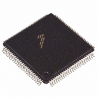
DSP56F803BU80 Freescale Semiconductor, DSP56F803BU80 Datasheet - Page 13

DSP56F803BU80
Manufacturer Part Number
DSP56F803BU80
Description
IC DSP 80MHZ 31.5K FLASH 100LQFP
Manufacturer
Freescale Semiconductor
Series
56F8xxr
Datasheet
1.DSP56F803BU80E.pdf
(52 pages)
Specifications of DSP56F803BU80
Core Processor
56800
Core Size
16-Bit
Speed
80MHz
Connectivity
CAN, EBI/EMI, SCI, SPI
Peripherals
POR, PWM, WDT
Number Of I /o
16
Program Memory Size
71KB (35.5K x 16)
Program Memory Type
FLASH
Ram Size
2.5K x 16
Voltage - Supply (vcc/vdd)
3 V ~ 3.6 V
Data Converters
A/D 8x12b
Oscillator Type
External
Operating Temperature
-40°C ~ 85°C
Package / Case
100-LQFP
Lead Free Status / RoHS Status
Contains lead / RoHS non-compliant
Eeprom Size
-
Available stocks
Company
Part Number
Manufacturer
Quantity
Price
Company:
Part Number:
DSP56F803BU80
Manufacturer:
MOTOLOLA
Quantity:
996
Company:
Part Number:
DSP56F803BU80
Manufacturer:
Freescale Semiconductor
Quantity:
10 000
Part Number:
DSP56F803BU80
Manufacturer:
FREESCALE
Quantity:
20 000
Company:
Part Number:
DSP56F803BU803
Manufacturer:
FREESCAL
Quantity:
329
Company:
Part Number:
DSP56F803BU80E
Manufacturer:
SHARP
Quantity:
5 600
Company:
Part Number:
DSP56F803BU80E
Manufacturer:
FREESCAL
Quantity:
364
Company:
Part Number:
DSP56F803BU80E
Manufacturer:
Freescale Semiconductor
Quantity:
10 000
Part Number:
DSP56F803BU80E
Manufacturer:
FREESCALE
Quantity:
20 000
2.6 Pulse Width Modulator (PWM) Signals
Freescale Semiconductor
No. of
No. of
Pins
Pins
6
3
3
1
1
FAULTA0
EXTBOOT
PWMA0
ISA0
RESET
Signal
Signal
Name
Name
–
Table 2-9 Interrupt and Program Control Signals (Continued)
2
–
–
5
2
(Schmitt)
(Schmitt)
Table 2-10 Pulse Width Modulator (PWMA) Signals
(Schmitt)
(Schmitt)
Signal
Signal
Output
Type
Input
Input
Type
Input
Input
State During
State During
Tri-stated
Reset
Reset
Input
Input
Input
Input
56F803 Technical Data, Rev. 16
PWMA0
ISA0
top/bottom pulse width correction in complementary channel
operation for PWMA.
FAULTA0
selected PWMA outputs in cases where fault conditions originate
off-chip.
Reset—This input is a direct hardware reset on the processor.
When RESET is asserted low, the controller is initialized and placed
in the Reset state. A Schmitt trigger input is used for noise immunity.
When the RESET pin is deasserted, the initial chip operating mode
is latched from the EXTBOOT pin. The internal reset signal will be
deasserted synchronous with the internal clocks, after a fixed
number of internal clocks.
To ensure a complete hardware reset, RESET and TRST should be
asserted together. The only exception occurs in a debugging
environment when a hardware device reset is required and it is
necessary not to reset the OnCE/JTAG module. In this case, assert
RESET, but do not assert TRST.
External Boot—This input is tied to V
off-chip memory. Otherwise, it is tied to V
–
2— These three input current status pins are used for
–
5— These are six PWMA output pins.
–
2— These three fault input pins are used for disabling
Signal Description
Signal Description
Pulse Width Modulator (PWM) Signals
DD
to force device to boot from
SS
.
13


