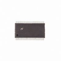
COP8CFE9IMT9/NOPB National Semiconductor, COP8CFE9IMT9/NOPB Datasheet - Page 14

COP8CFE9IMT9/NOPB
Manufacturer Part Number
COP8CFE9IMT9/NOPB
Description
IC MCU EEPROM 8BIT 8K 48-TSSOP
Manufacturer
National Semiconductor
Series
COP8™ 8Cr
Datasheet
1.COP8-EMFA-28N.pdf
(63 pages)
Specifications of COP8CFE9IMT9/NOPB
Core Processor
COP8
Core Size
8-Bit
Connectivity
Microwire/Plus (SPI)
Peripherals
POR, PWM, WDT
Number Of I /o
39
Program Memory Size
8KB (8K x 8)
Program Memory Type
FLASH
Ram Size
256 x 8
Voltage - Supply (vcc/vdd)
2.7 V ~ 5.5 V
Data Converters
A/D 16x10b
Oscillator Type
Internal
Operating Temperature
0°C ~ 70°C
Package / Case
48-TSSOP
Lead Free Status / RoHS Status
Lead free / RoHS Compliant
Speed
-
Eeprom Size
-
Other names
*COP8CFE9IMT9
*COP8CFE9IMT9/NOPB
COP8CFE9IMT9
*COP8CFE9IMT9/NOPB
COP8CFE9IMT9
www.national.com
3.0 Pin Descriptions
L3 Multi-Input Wake-up
L2 Multi-Input Wake-up
L1 Multi-Input Wake-up
L0 Multi-Input Wake-up
FIGURE 4. I/O Port Configurations — Output Mode
FIGURE 5. I/O Port Configurations — Input Mode
FIGURE 3. I/O Port Configurations
(Continued)
20026462
20026461
20026460
14
3.1 EMULATION CONNECTION
Connection to the emulation system is made via a 2 x 7
connector which interrupts the continuity of the RESET, G0,
G1, G2 and G3 signals between the COP8 device and the
rest of the target system (as shown in Figure 6 ). This con-
nector can be designed into the production pc board and can
be replaced by jumpers or signal traces when emulation is
no longer necessary. The emulator will replicate all functions
of G0 - G3 and RESET. For proper operation, no connection
should be made on the device side of the emulator connec-
tor.
4.0 Functional Description
The architecture of the device is a modified Harvard archi-
tecture. With the Harvard architecture, the program memory
(Flash) is separate from the data store memory (RAM). Both
Program Memory and Data Memory have their own separate
addressing space with separate address buses. The archi-
tecture, though based on the Harvard architecture, permits
transfer of data from Flash Memory to RAM.
4.1 CPU REGISTERS
The CPU can do an 8-bit addition, subtraction, logical or shift
operation in one instruction (t
There are six CPU registers:
A is the 8-bit Accumulator Register
PC is the 15-bit Program Counter Register
B is an 8-bit RAM address pointer, which can be optionally
post auto incremented or decremented.
X is an 8-bit alternate RAM address pointer, which can be
optionally post auto incremented or decremented.
S is the 8-bit Data Segment Address Register used to extend
the lower half of the address range (00 to 7F) into 256 data
segments of 128 bytes each.
SP is the 8-bit stack pointer, which points to the subroutine/
interrupt stack (in RAM). With reset the SP is initialized to
PU is the upper 7 bits of the program counter (PC)
PL is the lower 8 bits of the program counter (PC)
FIGURE 6. Emulation Connection
C
) cycle time.
20026409


