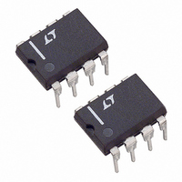
LT1112CN8#PBF Linear Technology, LT1112CN8#PBF Datasheet - Page 11

LT1112CN8#PBF
Manufacturer Part Number
LT1112CN8#PBF
Description
IC PREC OP-AMP LOWPWR DUAL 8-DIP
Manufacturer
Linear Technology
Datasheet
1.LT1112CN8PBF.pdf
(16 pages)
Specifications of LT1112CN8#PBF
Amplifier Type
General Purpose
Number Of Circuits
2
Slew Rate
0.3 V/µs
Gain Bandwidth Product
750kHz
Current - Input Bias
80pA
Voltage - Input Offset
25µV
Current - Supply
350µA
Voltage - Supply, Single/dual (±)
2 V ~ 40 V, ±1 V ~ 20 V
Operating Temperature
0°C ~ 70°C
Mounting Type
Through Hole
Package / Case
8-DIP (0.300", 7.62mm)
Lead Free Status / RoHS Status
Lead free / RoHS Compliant
Output Type
-
Current - Output / Channel
-
-3db Bandwidth
-
Available stocks
Company
Part Number
Manufacturer
Quantity
Price
APPLICATIO S I FOR ATIO
IN
IN
The concepts of common mode and power supply rejec-
tion ratio match (∆CMRR and ∆PSRR) are best demon-
strated with a numerical example:
Clearly the LT1112/LT1114, by specifying and guarantee-
ing all of these matching parameters, can significantly
improve the performance of matching-dependent
circuits.
–
+
Assume CMRR
and CMRR
then ∆CMRR = 0.25µV/V or 132dB;
if CMRR
then ∆CMRR = 1.75µV/V or 115dB.
1/2 LT1112
1/4 LT1114
1/2 LT1112
1/4 LT1114
+
–
–
+
OR
OR
D
A
Three Op Amp Instrumentation Amplifier
B
= – 0.75µV/V which is still 122.5dB,
B
= + 0.75µV/V or 122.5dB,
A
U
R1
10k
1%
R3
2.1k
1%
R8
200Ω
R2
10k
1%
= + 1µV/V or 120dB,
100Ω
100Ω
0.5%
0.5%
R4
R5
U
C1
33pF
R10
1M
R7
9.88k
0.5%
R9
200Ω
W
LT1097 OR
0.5%
–
1/4LT1114
+
10k
R6
B OR C
GAIN = 1000
TRIM R8 FOR GAIN
TRIM R9 FOR DC
COMMON MODE REJECTION
TRIM R10 FOR AC
COMMON MODE REJECTION
U
LT1112/14 • AI02
OUTPUT
Typical performance of the instrumentation amplifier:
When the instrumentation amplifier is used with high
impedance sources, the LT1114 is recommended because
its CMRR vs frequency performance is better than the
LT1112’s. For example, with two matched 1MΩ source
resistors, CMRR at 100Hz is 100dB with the LT1114, 76dB
with the LT1112.
This difference is explained by the fact that capacitance
between adjacent pins on an IC package is about 0.25pF
(including package, socket and PC board trace capaci-
tances).
On the dual op amp package, positive input A is next to the
V
ground pin adjacent to it, resulting in a 0.25pF input
capacitance mismatch. At 100Hz, 0.25pF represents a
6.4 • 10
higher than the 1MΩ source resistors.
On the quad package, all four inputs are adjacent to a
power supply terminal—therefore, there is no mismatch.
–
Input offset voltage = 35µV
Offset voltage drift = 0.3µV/°C
Input bias current = 80pA
Input offset current = 100pA
Input resistance = 800GΩ
Input noise = 0.42µV
pin (AC ground), while positive input B has no AC
9
input impedance mismatch, which is only 76dB
P-P
LT1112/LT1114
11
111214fb


