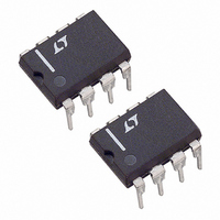
LT1112CN8#PBF Linear Technology, LT1112CN8#PBF Datasheet - Page 6

LT1112CN8#PBF
Manufacturer Part Number
LT1112CN8#PBF
Description
IC PREC OP-AMP LOWPWR DUAL 8-DIP
Manufacturer
Linear Technology
Datasheet
1.LT1112CN8PBF.pdf
(16 pages)
Specifications of LT1112CN8#PBF
Amplifier Type
General Purpose
Number Of Circuits
2
Slew Rate
0.3 V/µs
Gain Bandwidth Product
750kHz
Current - Input Bias
80pA
Voltage - Input Offset
25µV
Current - Supply
350µA
Voltage - Supply, Single/dual (±)
2 V ~ 40 V, ±1 V ~ 20 V
Operating Temperature
0°C ~ 70°C
Mounting Type
Through Hole
Package / Case
8-DIP (0.300", 7.62mm)
Lead Free Status / RoHS Status
Lead free / RoHS Compliant
Output Type
-
Current - Output / Channel
-
-3db Bandwidth
-
Available stocks
Company
Part Number
Manufacturer
Quantity
Price
LT1112/LT1114
ELECTRICAL CHARACTERISTICS
Note 5: Offset voltage, supply current and power supply rejection ratio are
measured at the minimum supply voltage.
Note 6: Matching parameters are the difference between amplifiers A and
D and between B and C on the LT1114; between the two amplifiers on the
LT1112.
Note 7: This parameter is the difference between two noninverting input
bias currents.
Note 8: ∆CMRR and ∆PSRR are defined as follows: (1) CMRR and PSRR
are measured in µV/V on the individual amplifiers. (2) The difference is
calculated between the matching sides in µV/V. (3) The result is converted
to dB.
Note 9: This parameter is not 100% tested.
6
TYPICAL PERFOR A CE CHARACTERISTICS
–100
–200
100
200
OFFSET VOLTAGE DRIFT WITH TEMPERATURE (µV/°C)
15
10
20
0
0
5
–0.8
–75
Input Bias and Offset Current,
Noninverting Bias Current Match
vs Temperature
Drift with Temperature
LT1112N8/J8, LT1114J
850 OP AMPS TESTED
100 LT1112J8
165 LT1112N8
80 LT1114J
V
S
–0.6
–50 –25
= ±15V
–0.4
I
B
TEMPERATURE (°C)
(OVERCANCELLED)
–0.2
0
I
B
(UNDERCANCELLED)
25
0
0.2
50
75
0.4
W
LT1112/14 • TPC04
V
LT1112/14 • TPC01
∆I
S
B
= ±15V
100 125
+
0.6
I
OS
U
0.8
–100
–150
150
100
–50
50
15
OFFSET VOLTAGE DRIFT WITH TEMPERATURE (µV/°C)
25
20
10
0
0
5
–15
–1.4
Input Bias Current Over
Common Mode Range
Drift with Temperature
LT1112S8, LT1114N/S
960 OP AMPS TESTED
240 LT1112S8
80 LT1114N
40 LT1114S
V
T
R
S
A
INCM
DEVICE WITH POSITIVE INPUT CURRENT
DEVICE WITH NEGATIVE INPUT CURRENT
= 25°C
COMMON MODE INPUT VOLTAGE (V)
–1.0
= ±15V
–10
= 800GΩ
–0.6
–5
–0.2
Note 10: These parameters are not tested. More than 99% of the op amps
tested during product characterization have passed the maximum limits.
100% passed at 1kHz.
Note 11: The LT1112AC/LT1112C/LT1112S8/LT1112I and LT1114AC/
LT1114C/LT1114S/LT1114I are guaranteed functional over the
temperature range of –40°C to 85°C.
Note 12: The LT1112AC/LT1112C/LT1112S8/LT1114AC/LT1114C/
LT1114S are guaranteed to meet specified performance from 0°C to 70°C
and are designed, characterized and expected to meet specified
performance from –40°C to 85°C, but are not tested or QA sampled at
these temperatures. The LT1112I/LT1114I are guaranteed to meet
specified performance from –40°C to 85°C.
0
V CM
0.2
I
B
5
0.6
–
+
V
LT1112/14 • TPC02
LT1112/14 • TPC05
S
= ±15V
10
1.0
1.4
15
30
20
10
20
10
30
25
15
0
0
5
–300
–80
Distribution of Input Bias Current
(In All Packages Except LT1114S)
Distribution of Offset Voltage at
V
S
V
T
T
A
S
A
–60
= ±1.0V (In All Packages)
= 25°C
= ±15V
= 25°C
–200 –100
–40
INPUT OFFSET VOLTAGE (µV)
INPUT BIAS CURRENT (pA)
–20
0
0
20
100
40
LT1112/14 • TPC06
60
LT1112/14 • TPC03
200
111214fb
80
300
100


