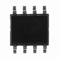
CS3011-ISZ Cirrus Logic Inc, CS3011-ISZ Datasheet - Page 13

CS3011-ISZ
Manufacturer Part Number
CS3011-ISZ
Description
IC OPAMP SGL PREC LV 8-SOIC
Manufacturer
Cirrus Logic Inc
Datasheet
1.CS3011-ISZ.pdf
(18 pages)
Specifications of CS3011-ISZ
Amplifier Type
Instrumentation
Number Of Circuits
1
Output Type
Rail-to-Rail
Slew Rate
2 V/µs
Current - Input Bias
50pA
Voltage - Input Offset
10µV
Current - Supply
900µA
Voltage - Supply, Single/dual (±)
2.7 V ~ 6.7 V, ±1.35 V ~ 3.35 V
Operating Temperature
-40°C ~ 85°C
Mounting Type
Surface Mount
Package / Case
8-SOIC
Number Of Channels
1
Voltage Gain Db
300 dB
Common Mode Rejection Ratio (min)
115 dB
Input Offset Voltage
0.01 mV
Operating Supply Voltage
2.7 V to 6.7 V
Supply Current
0.9 mA
Maximum Operating Temperature
+ 85 C
Mounting Style
SMD/SMT
Maximum Dual Supply Voltage
+/- 3.35 V
Minimum Operating Temperature
- 40 C
For Use With
598-1495 - BOARD EVAL OPAMP FOR CS30XX
Lead Free Status / RoHS Status
Lead free / RoHS Compliant
Current - Output / Channel
-
-3db Bandwidth
-
Gain Bandwidth Product
-
Lead Free Status / Rohs Status
Details
Other names
598-1142-5
3.2.2
Condition #1: |Av| ≤ 50 and R1 ≤ 100 Ω
The Opamp is inheren tly stable for |Av| ≤ 50 an d
R1 ≤ 100 Ω . No
across R2 is required.
•
•
Condition #2: |Av| ≤ 50 and R1 > 100 Ω
Compensation capacitor C2 across R2 is required.
Calculate C2 using the following formula:
•
Condition #3: |Av| > 50
Compensation capacitor C2 across R2 is required.
Calculate and verify a value for C2 using the fol-
lowing steps.
Calculate the Compensation Capacitor Value:
1) Calculate a value for C2 using the following for-
To simplify the calculation, set the pole of the filter
to P1 = 1 MHz. P1 must be set h igher than the
opamp’s internal 50 kHz crossover frequency.
2) Calculate a second value for C2 using the fol-
3) Use the la rger of t he two va lues calculated in
DS597F6
|Av| = 1 config uration ha s 7 0° pha se margin
and 20 dB gain margin.
|Av| = 50 configuration ha s p hase ma rgin be-
tween 40° for C
C
C2 ≥ (R1 • C
mula:
C2 = 1 / [2π (R1| |R2) • P1], where P1 = 1 MHz
lowing formula:
C2 ≥ (R1 • C
steps 1 & 2.
LOAD
Gain Calculations Summary and
Recommendations
= 0 pF.
in
in
) / R2, where Cin = 50 pF
) / R2, where Cin = 50 pF
C2 co mpensation cap acitor
LOAD
≤ 100 pF and 60 ° for
Verify the Opamp Compensation:
Verify the opamp co mpensation using the ope n-
loop gain and pha se resp onse Bode plot
Figure 14.
transfer function and verify the following design cri-
teria are met:
•
•
•
3.3
The CS3011 single amplifier provides a power-
down function on pin 1. If this pin is left ope n the
amplifier will operate normally. If the powerdown is
asserted low, the amplifier enters a powered down
state. Th ere is a pu ll-up resistor (approximately
800 k ohm) inside the amplifier from pin 1 to the V+
supply. The current through this pull-up resistor is
the main source of current drain in the powerdown
state.
-
-
-
Pole P1 > opamp in ternal 50 kHz c rossover fre-
quency
Z1 < opamp internal 50 kHz crossover frequency
Gain margin above the open-loop gain transfer
function is re quired. A g ain margin of +2 0 dB
above t he op en loop g ain transfer fun ction is
optimal.
P1 = 1 / [2π (R1| |R2) • C2], where P1 = 1 MHz
To sim plify the ca lculation, set t he p ole t o
P1 = 1 MHz.
Z1 = 1 / (2π R2 • C2)
Powerdown (PDWN)
Plot the calculated clo sed loop gain
CS3012
CS3011
13
in


