AD704JNZ Analog Devices Inc, AD704JNZ Datasheet - Page 2
AD704JNZ
Manufacturer Part Number
AD704JNZ
Description
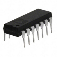
IC OPAMP GP QUAD PREC LN 14DIP
Manufacturer
Analog Devices Inc
Specifications of AD704JNZ
Slew Rate
0.15 V/µs
Amplifier Type
General Purpose
Number Of Circuits
4
-3db Bandwidth
800kHz
Current - Input Bias
100pA
Voltage - Input Offset
50µV
Current - Supply
1.5mA
Current - Output / Channel
15mA
Voltage - Supply, Single/dual (±)
4 V ~ 36 V, ±2 V ~ 18 V
Operating Temperature
0°C ~ 70°C
Mounting Type
Through Hole
Package / Case
14-DIP (0.300", 7.62mm)
Op Amp Type
Precision
No. Of Amplifiers
4
Bandwidth
800kHz
Supply Voltage Range
± 2V To ± 18V
Amplifier Case Style
DIP
No. Of Pins
14
Common Mode Rejection Ratio
100
Current, Input Bias
270 pA
Current, Input Offset
1 pA
Current, Supply
600 μA
Number Of Amplifiers
Quad
Package Type
PDIP-14
Power Dissipation
650 mW
Temperature, Operating, Range
-55 to +125 °C
Voltage, Gain
200 V/mV
Voltage, Input
±18 V
Voltage, Noise
15 nV/sqrt Hz
Voltage, Offset
150 μV
Voltage, Output, High
+13 V
Voltage, Output, Low
-13 V
Voltage, Supply
±18 V
Lead Free Status / RoHS Status
Lead free / RoHS Compliant
Output Type
-
Gain Bandwidth Product
-
Lead Free Status / Rohs Status
RoHS Compliant part
Electrostatic Device


AD704/883B
Test
Input Offset Voltage
Power Supply Rejection Ratio
Input Bias Current
Input Offset Current
Matching Characteristics
Common-Mode Rejection Ratio
Open-Loop Gain
Output Voltage Swing
Power Supply Quiescent Current
1
2
3
4
5
Bias current specifications maximum at either input.
Input bias current match is the maximum difference between the corresponding inputs of all four amplifiers.
CMR match is the difference between ΔV
PSR match is the difference between ΔV
V
Offset Voltage
Input Bias Current
Common-Mode Rejection
Power Supply Rejection
S
= ±15 V, unless otherwise noted.
2
3
5
4
OS
OS
/ΔV
/ΔV
SUPPLY
CM
for any two amplifiers, expressed in dB.
for any two amplifiers, expressed in dB.
Symbol
V
PSRR
I
I
V
I
CMR
PSR
CMRR
A
V
I
B
OS
B
Q
OS
OS
OL
OUT
1
Sub Group
1
2, 3
1
2, 3
1
2, 3
1
2, 3
1
2, 3
1
2, 3
1
2, 3
1
2, 3
1, 2, 3
1, 2, 3
2, 3
1
2, 3
1
2, 3
1, 2, 3
1
2, 3
Rev. C | Page 2 of 3
Table 1.
Min
100
100
94
94
100
98
200
150
200
100
±13
Limits
Max
270
300
300
2.5
150
250
600
700
250
400
500
250
400
500
600
2.8
Unit
μV
dB
pA
pA
pA
pA
μV
pA
dB
dB
dB
V/mV
V/mV
V
mA
Test Conditions
±2 V ≤ V
±2.5 V ≤ V
Either input, V
Either input, V
V
V
V
V
V
R
L
CM
CM
CM
O
O
= 10 kΩ
= ±12 V, R
= ±10 V, R
= 0 V
= ±13.5 V
= ±13.5 V
S
≤ ±18 V
S
≤ ±18 V
L
L
CM
CM
= 10 kΩ
= 2 kΩ
1
= 0 V
= ±13.5 V
Related parts for AD704JNZ
Image
Part Number
Description
Manufacturer
Datasheet
Request
R

Part Number:
Description:
±1.7g Dual-Axis IMEMS Accelerometer Evaluation Board
Manufacturer:
Analog Devices Inc
Datasheet:

Part Number:
Description:
Inertial Sensor Evaluation System
Manufacturer:
Analog Devices Inc
Datasheet:
Part Number:
Description:
Manufacturer:
Analog Devices Inc
Datasheet:
Part Number:
Description:
Manufacturer:
Analog Devices Inc
Datasheet:
Part Number:
Description:
Manufacturer:
Analog Devices Inc
Datasheet:
Part Number:
Description:
Manufacturer:
Analog Devices Inc
Datasheet:
Part Number:
Description:
Manufacturer:
Analog Devices Inc
Datasheet:
Part Number:
Description:
Manufacturer:
Analog Devices Inc
Datasheet:
Part Number:
Description:
Manufacturer:
Analog Devices Inc
Datasheet:
Part Number:
Description:
Manufacturer:
Analog Devices Inc
Datasheet:
Part Number:
Description:
Manufacturer:
Analog Devices Inc
Datasheet:
Part Number:
Description:
Manufacturer:
Analog Devices Inc
Datasheet:
Part Number:
Description:
Manufacturer:
Analog Devices Inc
Datasheet: