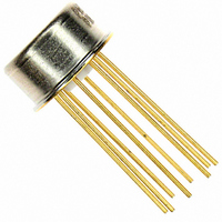
AD549JHZ Analog Devices Inc, AD549JHZ Datasheet

AD549JHZ
Specifications of AD549JHZ
Available stocks
Related parts for AD549JHZ
AD549JHZ Summary of contents
Page 1
FEATURES Ultralow input bias current 60 fA maximum (AD549L) 250 fA maximum (AD549J) Input bias current guaranteed over the common-mode voltage range Low offset voltage 0.25 mV maximum (AD549K) 1.00 mV maximum (AD549J) Low offset drift 5 μV/°C maximum (AD549K) ...
Page 2
AD549 TABLE OF CONTENTS Features .............................................................................................. 1 Applications ....................................................................................... 1 Connection Diagram ....................................................................... 1 General Description ......................................................................... 1 Product Highlights ........................................................................... 1 Revision History ............................................................................... 2 Specifications ..................................................................................... 3 Absolute Maximum Ratings ............................................................ 5 ESD Caution .................................................................................. 5 Typical Performance ...
Page 3
SPECIFICATIONS @ 25°C and V = ±15 V dc, unless otherwise noted; all minimum and maximum specifications are guaranteed; specifications in boldface S are tested on all production units at final electrical test, and results from those tests are used ...
Page 4
AD549 AD549J Parameter Min Typ OUTPUT CHARACTERISTICS kΩ −12 OUT L MIN T MAX kΩ −10 OUT L MIN MAX Short-Circuit Current ...
Page 5
ABSOLUTE MAXIMUM RATINGS Table 2. Parameter Supply Voltage Internal Power Dissipation 1 Input Voltage Output Short-Circuit Duration Differential Input Voltage Storage Temperature Range Operating Temperature Range AD549J, AD549K, AD549L AD549S Lead Temperature (Soldering, 60 sec) 1 For supply voltages less ...
Page 6
AD549 TYPICAL PERFORMANCE CHARACTERISTICS IN SUPPLY VOLTAGE (±V) Figure 2. Input Voltage Range vs. Supply Voltage 20 25° 10kΩ SUPPLY VOLTAGE ...
Page 7
TEMPERATURE (°C) Figure 8. Open-Loop Gain vs. Temperature WARM-UP TIME (Minutes) Figure 9. Change in Offset Voltage vs. ...
Page 8
AD549 100 –20 –40 10 100 1k 10k 100k FREQUENCY (Hz) Figure 14. Open-Loop Frequency Response 100 1k 10k FREQUENCY (Hz) Figure 15. Large Signal ...
Page 9
S 0.1µ AD549 10kΩ 100pF 3 IN 0.1µF SQUARE WAVE –V S INPUT Figure 19. Unity-Gain Follower 5V 5µs Figure 20. Unity-Gain Follower Large Signal Pulse Response 10mV 1µs Figure ...
Page 10
AD549 FUNCTIONAL DESCRIPTION MINIMIZING INPUT CURRENT The AD549 is optimized for low input current and offset voltage. Careful attention to how the amplifier is used reduces input currents in actual applications. Keep the amplifier operating temperature as low as possible ...
Page 11
The case of the AD549 is connected to Pin 8 so that it can be bootstrapped near the input potential. This minimizes pin leakage and input common-mode capacitance due to the case. Guard schemes for inverting and noninverting amplifier topologies ...
Page 12
AD549 AC RESPONSE WITH HIGH VALUE SOURCE AND FEEDBACK RESISTANCE Source and feedback resistances greater than 100 kΩ magnify the effect of the input capacitances (stray and inherent to the AD549) on the ac behavior of the circuit. The effects ...
Page 13
DIFFERENTIAL INPUT VOLTAGE OVERLOAD A plot of the AD549 input currents vs. differential input voltage (defined as V − appears in Figure 36. The IN+ IN− input current at either terminal stays below a few hundred femtoamps until ...
Page 14
AD549 The test apparatus is calibrated without a device under test present. After power is turned on minute stabilization period is required. First, V and V ERR1 ERR2 voltages are the errors caused by the offset voltages and ...
Page 15
Input current contributes an output voltage error proportional to the feedback resistance × The input voltage offset of the op amp causes an error current through the photodiode shunt ...
Page 16
AD549 Frequency compensation is provided by R11, R12, C1, and C2. The bandwidth of the circuit is 300 kHz at input signals greater than 50 μA; bandwidth decreases smoothly with decreasing signal levels. To trim the circuit, set the input ...
Page 17
The pH probe output is ideally independent of temperature. The slope of the transfer function of the probe, though predictable, is temperature dependent (−54.2 mV/pH at 0°C and −74.04 mV/pH at 100°C). By ...
Page 18
... PARENTHESES) ARE ROUNDED-OFF INCH EQUIVALENTS FOR REFERENCE ONLY AND ARE NOT APPROPRIATE FOR USE IN DESIGN. ORDERING GUIDE Model Temperature Range AD549JH 0°C to +70°C 1 AD549JHZ 0°C to +70°C AD549KH 0°C to +70°C 1 AD549KHZ 0°C to +70°C AD549LH 0°C to +70°C ...
Page 19
NOTES Rev Page AD549 ...
Page 20
AD549 NOTES ©2002–2008 Analog Devices, Inc. All rights reserved. Trademarks and registered trademarks are the property of their respective owners. D00511-0-3/08(H) Rev Page ...


