AD549LHZ Analog Devices Inc, AD549LHZ Datasheet - Page 14
AD549LHZ
Manufacturer Part Number
AD549LHZ
Description
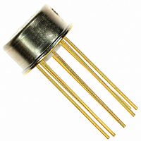
IC OPAMP GP 1MHZ LP 20MA TO99-8
Manufacturer
Analog Devices Inc
Series
Topgate™r
Datasheet
1.AD549JHZ.pdf
(20 pages)
Specifications of AD549LHZ
Slew Rate
3 V/µs
Amplifier Type
General Purpose
Number Of Circuits
1
Gain Bandwidth Product
1MHz
Current - Input Bias
0.04pA
Voltage - Input Offset
300µV
Current - Supply
600µA
Current - Output / Channel
20mA
Voltage - Supply, Single/dual (±)
±5 V ~ 18 V
Operating Temperature
0°C ~ 70°C
Mounting Type
Through Hole
Package / Case
TO-99-8, Metal Can
Op Amp Type
Low Bias Current
No. Of Amplifiers
1
Bandwidth
1MHz
Supply Voltage Range
± 5V To ± 18V
Amplifier Case Style
TO-99
No. Of Pins
8
Lead Free Status / RoHS Status
Lead free / RoHS Compliant
Output Type
-
-3db Bandwidth
-
Lead Free Status / Rohs Status
RoHS Compliant part
Electrostatic Device
Available stocks
Company
Part Number
Manufacturer
Quantity
Price

Part Number:
AD549LHZ
Manufacturer:
ADI/亚德诺
Quantity:
20 000


AD549
The test apparatus is calibrated without a device under test
present. After power is turned on, a 5 minute stabilization
period is required. First, V
voltages are the errors caused by the offset voltages and leakage
currents of the I-to-V converters.
Once measured, these errors are subtracted from the readings
taken with a device under test present. Amplifier B closes the
feedback loop to the device under testing in addition to pro-
viding the I-to-V conversion. The offset error of the device
under testing appears as a common-mode signal and does not
affect the test measurement. As a result, only the leakage
current of the device under testing is measured.
V
V
V
V
V
ERR1
ERR2
A
X
OS
– V
– V
–
+
I (+)
I (–)
Figure 40. Sample and Difference Circuit for Measuring
= 10 (V
= 10 (V
ERR1
ERR2
DEVICE
= 10[RSa × I
= 10[RSb × I
UNDER
TEST
OS
OS
Electrometer Leakage Currents
A – I
B – I
9.01kΩ
B
B
1kΩ
B × RSb)
A × RSa)
R2
R1
ERR1
B
B
(+)]
(–)]
and V
10
10
20pF
20pF
RSa
RSb
C
2
3
3
2
C
10
10
C
C
Ω
AD549
AD549
Ω
ERR2
A
B
8
8
are measured. These
R1
1kΩ
R1
1kΩ
C
0.1µF
GUARD
9.01kΩ
9.01kΩ
F
0.1µF
0.1µF
C
R2
C
R2
F
F
6
6
V
V
ERR1
ERR2
V
OUT
CAL/TEST
/V
–
/V
+
+
–
A
B
Rev. H | Page 14 of 20
Although a series of devices can be tested after only one calibra-
tion measurement, calibration should be updated periodically
to compensate for any thermal drift of the I-to-V converters or
changes in the ambient environment. Laboratory results have
shown that repeatable measurements within 10 fA can be realized
when this apparatus is properly implemented. These results are
achieved in part by the design of the circuit, which eliminates
relays and other parasitic leakage paths in the high impedance
signal lines, and in part by the inherent cancellation of errors
through the calibration and measurement procedure.
PHOTODIODE INTERFACE
The low input current and low input offset voltage of the AD549
make it an excellent choice for very sensitive photodiode preamps
(see Figure 41). The photodiode develops a signal current, I
equal to
where P is light power incident on the diode surface, in watts,
and R is the photodiode responsivity in amps/watt. R
the signal current to an output voltage
The dc error sources and an equivalent circuit for a small area
(0.2 mm square) photodiode are indicated in Figure 42.
I
S
I
V
S
OUT
= R × P
10
I
S
= R
R
9
Ω
S
Figure 42. Photodiode Preamp DC Error Sources
F
× I
20pF
C
S
S
Figure 41. Photodiode Preamp
2
3
AD549
–V
I
4
S
S
–
1
10
10pF
R
C
–
9
F
F
Ω
5
V
OS
6
10
R
+
9
F
Ω
A
10kΩ
1µF
10pF
C
F
+
–
V
OUT
F
converts
V
OUT
+
–
S
,
Related parts for AD549LHZ
Image
Part Number
Description
Manufacturer
Datasheet
Request
R

Part Number:
Description:
±1.7g Dual-Axis IMEMS Accelerometer Evaluation Board
Manufacturer:
Analog Devices Inc
Datasheet:

Part Number:
Description:
Inertial Sensor Evaluation System
Manufacturer:
Analog Devices Inc
Datasheet:
Part Number:
Description:
Manufacturer:
Analog Devices Inc
Datasheet:
Part Number:
Description:
Manufacturer:
Analog Devices Inc
Datasheet:
Part Number:
Description:
Manufacturer:
Analog Devices Inc
Datasheet:
Part Number:
Description:
Manufacturer:
Analog Devices Inc
Datasheet:
Part Number:
Description:
Manufacturer:
Analog Devices Inc
Datasheet:
Part Number:
Description:
Manufacturer:
Analog Devices Inc
Datasheet:
Part Number:
Description:
Manufacturer:
Analog Devices Inc
Datasheet:
Part Number:
Description:
Manufacturer:
Analog Devices Inc
Datasheet:
Part Number:
Description:
Manufacturer:
Analog Devices Inc
Datasheet:
Part Number:
Description:
Manufacturer:
Analog Devices Inc
Datasheet:
Part Number:
Description:
Manufacturer:
Analog Devices Inc
Datasheet: