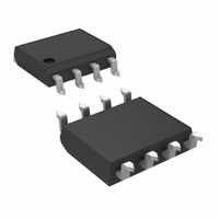
LF353MX/NOPB National Semiconductor, LF353MX/NOPB Datasheet

LF353MX/NOPB
Specifications of LF353MX/NOPB
LF353MXTR
Available stocks
Related parts for LF353MX/NOPB
LF353MX/NOPB Summary of contents
Page 1
... The devices also exhibit low noise and offset voltage drift. Typical Connection Simplified Schematic 1/2 Dual BI-FET II ™ trademark of National Semiconductor Corporation. © 2003 National Semiconductor Corporation Features n Internally trimmed offset voltage: n Low input bias current: n Low input noise voltage: n Low input noise current: ...
Page 2
... Absolute Maximum Ratings If Military/Aerospace specified devices are required, please contact the National Semiconductor Sales Office/ Distributors for availability and specifications. Supply Voltage Power Dissipation Operating Temperature Range T (MAX) j Differential Input Voltage Input Voltage Range (Note 3) Output Short Circuit Duration Storage Temperature Range Lead Temp ...
Page 3
AC Electrical Characteristics (Note 5) Symbol Parameter THD Total Harmonic Distortion Note 2: For operating at elevated temperatures, the device must be derated based on a thermal resistance of 115˚C/W typ junction to ambient for the N package, and 158˚C/W ...
Page 4
Typical Performance Characteristics Negative Common-Mode Input Voltage Limit Negative Current Limit Output Voltage Swing www.national.com (Continued) Positive Current Limit 00564922 00564924 00564926 4 00564923 Voltage Swing 00564925 Gain Bandwidth 00564927 ...
Page 5
Typical Performance Characteristics Bode Plot Distortion vs. Frequency Open Loop Frequency Response (Continued) 00564928 Undistorted Output Voltage Swing 00564930 Common-Mode Rejection Ratio 00564932 5 Slew Rate 00564929 00564931 00564933 www.national.com ...
Page 6
Typical Performance Characteristics Power Supply Rejection Ratio Open Loop Voltage Gain (V/V) Inverter Settling Time www.national.com (Continued) Equivalent Input Noise Voltage 00564934 Output Impedance 00564936 00564938 6 00564935 00564937 ...
Page 7
Pulse Response Small Signaling Inverting Large Signal Inverting Application Hints These devices are op amps with an internally trimmed input offset voltage and JFET input devices (BI-FET II). These JFETs have large reverse breakdown voltages from gate to source and ...
Page 8
Application Hints (Continued) since raising the input back within the common-mode range again puts the input stage and thus the amplifier in a normal operating mode. Exceeding the positive common-mode limit on a single input will not change the phase ...
Page 9
Typical Applications Note 1: All controls flat. Note 2: Bass and treble boost, mid flat. Note 3: Bass and treble cut, mid flat. Note 4: Mid boost, bass and treble flat. Note 5: Mid cut, bass and treble flat. • ...
Page 10
Typical Applications www.national.com (Continued) Improved CMRR Instrumentation Amplifier Fourth Order Low Pass Butterworth Filter 10 00564941 00564942 ...
Page 11
Typical Applications (Continued) Fourth Order High Pass Butterworth Filter 11 00564943 www.national.com ...
Page 12
Typical Applications www.national.com (Continued) Ohms to Volts Converter 12 00564944 ...
Page 13
Physical Dimensions inches (millimeters) unless otherwise noted Order Number LF353M or LF353MX NS Package Number M08A Molded Dual-In-Line Package Order Number LF353N NS Package N08E 13 www.national.com ...
Page 14
... BANNED SUBSTANCE COMPLIANCE National Semiconductor certifies that the products and packing materials meet the provisions of the Customer Products Stewardship Specification (CSP-9-111C2) and the Banned Substances and Materials of Interest Specification (CSP-9-111S2) and contain no ‘‘Banned Substances’’ as defined in CSP-9-111S2. ...


