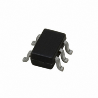
LPV511MG/NOPB National Semiconductor, LPV511MG/NOPB Datasheet - Page 11

LPV511MG/NOPB
Manufacturer Part Number
LPV511MG/NOPB
Description
IC OP AMP 880NA R-R SC70-5
Manufacturer
National Semiconductor
Series
PowerWise®r
Datasheet
1.LPV511MGNOPB.pdf
(14 pages)
Specifications of LPV511MG/NOPB
Amplifier Type
General Purpose
Number Of Circuits
1
Output Type
Rail-to-Rail
Slew Rate
0.0077 V/µs
Gain Bandwidth Product
25kHz
Current - Input Bias
320pA
Voltage - Input Offset
200µV
Current - Supply
1.2µA
Current - Output / Channel
1.3mA
Voltage - Supply, Single/dual (±)
2.7 V ~ 12 V
Operating Temperature
-40°C ~ 85°C
Mounting Type
Surface Mount
Package / Case
SC-70-5, SC-88A, SOT-323-5, SOT-353, 5-TSSOP
Number Of Channels
1
Voltage Gain Db
110 dB
Common Mode Rejection Ratio (min)
80 dB
Input Voltage Range (max)
12 V
Input Voltage Range (min)
2.7 V
Input Offset Voltage
3 mV at 5 V
Operating Supply Voltage
3 V, 5 V, 9 V
Supply Current
0.0012 mA at 5 V
Maximum Operating Temperature
+ 85 C
Mounting Style
SMD/SMT
Minimum Operating Temperature
- 40 C
Lead Free Status / RoHS Status
Lead free / RoHS Compliant
-3db Bandwidth
-
Lead Free Status / Rohs Status
Details
Other names
LPV511MG
LPV511MGNOPB
LPV511MGNOPBTR
LPV511MGNOPBTR
LPV511MGTR
LPV511MGNOPB
LPV511MGNOPBTR
LPV511MGNOPBTR
LPV511MGTR
Application Notes
The LPV511 is fabricated with National Semiconductor's
state-of-the-art VIP50C process.
INPUT STAGE
The LPV511 has a rail-to-rail input which provides more flex-
ibility for the system designer. As can be seen from the
simplified schematic, rail-to-rail input is achieved by using in
parallel, one PNP differential pair and one NPN differential
pair. When the common mode input voltage (V
+
near V
V
current each differential pair will get. This special logic en-
sures stable and low distortion amplifier operation within the
entire common mode voltage range.
Because both input stages have their own offset voltage
(V
comes a function of V
below V
formance Characteristics section. Caution should be taken in
situations where the input signal amplitude is comparable to
the V
these situations, it is necessary for the input signal to avoid
the crossover point.
The input bias current, I
the input crosses the transition region. In addition, parameters
such as PSRR and CMRR which involve the input offset volt-
age will also be affected by changes in V
ential pair transition region.
Differential input voltage is the difference in voltage between
the non-inverting (+) input and the inverting input (−) of the op
amp. Due to the three series diodes across the two inputs, the
absolute maximum differential input voltage is ±2.1V. This
may not be a problem to most conventional op amp designs;
however, designers should avoid using the LPV511 as a com-
parator.
OUTPUT STAGE
The LPV511 output voltage swing 100 mV from rails @ 3V
supply, which provides the maximum possible dynamic range
at the output. This is particularly important when operating on
low supply voltages.
The LPV511 Maximum Output Voltage Swing defines the
maximum swing possible under a particular output load. The
, the NPN pair is on and the PNP pair is off. When V
CM
OS
) characteristic, the offset voltage of the LPV511 be-
is between V
OS
−
, the NPN pair is off and the PNP pair is on. When
+
value and/or the design requires high accuracy. In
. Refer to the ’V
Inverting Small Signal Pulse Response
+
and V
CM
B
. V
OS
will change in value and polarity as
−
, internal logic decides how much
vs. V
OS
has a crossover point at 1.0V
CM
’ curve in the Typical Per-
CM
across the differ-
20117032
CM
) is near V
CM
is
11
LPV511 output swings 110 mV from the rail @ 5V supply with
an output load of 100 kΩ.
DRIVING CAPACITIVE LOAD
The LPV511 is internally compensated for stable unity gain
operation, with a 27 kHz typical gain bandwidth. However, the
unity gain follower is the most sensitive configuration to ca-
pacitive load. Direct capacitive loading reduces the phase
margin of the op amp. When the output is required to drive a
large capacitive load, greater than 100 pF, a small series re-
sistor at the output of the amplifier improves the phase margin
(see Figure 1).
In Figure 1 , the isolation resistor R
C
margin to the overall system. The desired performance de-
pends on the value of R
the more stable V
when the R
Figure 1, the output voltage would be divided by R
load resistor.
POWER SUPPLIES AND LAYOUT
The LPV511 operates from a single 2.7V to 12V power sup-
ply. It is recommended to bypass the power supplies with a
0.1 μF ceramic capacitor placed close to the V
Ground layout improves performance by decreasing the
amount of stray capacitance and noise at the op amp's inputs
and outputs. To decrease stray capacitance, minimize PC
board trace lengths and resistor leads, and place external
components close to the op amps's pins.
L
form a pole to increase stability by adding more phase
FIGURE 1. Resistive Isolation of Capacitive Load
Inverting Large Signal Pulse Response
ISO
gets bigger. If there were a load resistor in
OUT
will be. But the DC accuracy is degraded
ISO
. The bigger the R
ISO
and the load capacitor
20117033
ISO
resistor value,
20117025
+
and V
www.national.com
ISO
and the
−
pins.


