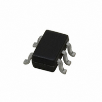
LPV511MG/NOPB National Semiconductor, LPV511MG/NOPB Datasheet - Page 2

LPV511MG/NOPB
Manufacturer Part Number
LPV511MG/NOPB
Description
IC OP AMP 880NA R-R SC70-5
Manufacturer
National Semiconductor
Series
PowerWise®r
Datasheet
1.LPV511MGNOPB.pdf
(14 pages)
Specifications of LPV511MG/NOPB
Amplifier Type
General Purpose
Number Of Circuits
1
Output Type
Rail-to-Rail
Slew Rate
0.0077 V/µs
Gain Bandwidth Product
25kHz
Current - Input Bias
320pA
Voltage - Input Offset
200µV
Current - Supply
1.2µA
Current - Output / Channel
1.3mA
Voltage - Supply, Single/dual (±)
2.7 V ~ 12 V
Operating Temperature
-40°C ~ 85°C
Mounting Type
Surface Mount
Package / Case
SC-70-5, SC-88A, SOT-323-5, SOT-353, 5-TSSOP
Number Of Channels
1
Voltage Gain Db
110 dB
Common Mode Rejection Ratio (min)
80 dB
Input Voltage Range (max)
12 V
Input Voltage Range (min)
2.7 V
Input Offset Voltage
3 mV at 5 V
Operating Supply Voltage
3 V, 5 V, 9 V
Supply Current
0.0012 mA at 5 V
Maximum Operating Temperature
+ 85 C
Mounting Style
SMD/SMT
Minimum Operating Temperature
- 40 C
Lead Free Status / RoHS Status
Lead free / RoHS Compliant
-3db Bandwidth
-
Lead Free Status / Rohs Status
Details
Other names
LPV511MG
LPV511MGNOPB
LPV511MGNOPBTR
LPV511MGNOPBTR
LPV511MGTR
LPV511MGNOPB
LPV511MGNOPBTR
LPV511MGNOPBTR
LPV511MGTR
www.national.com
V
TC V
I
I
CMRR
PSRR
CMVR
A
V
I
I
SR
B
OS
SC
S
Symbol
OS
VOL
O
Absolute Maximum Ratings
If Military/Aerospace specified devices are required,
please contact the National Semiconductor Sales Office/
Distributors for availability and specifications.
3V Electrical Characteristics
Unless otherwise specified, all limits are guaranteed for T
Boldface limits apply to the temperature range of −40°C to 85°C.
ESD Tolerance (Note 2)
V
Supply Voltage (V
Voltage at Input/Output pins
Storage Temperature Range
Short Circuit Duration
IN
OS
Human Body
Machine Model
Differential
Input Offset Voltage
Input Offset Voltage Drift
Input Bias Current (Note 9)
Input Offset Current
Common Mode Rejection Ratio
Power Supply Rejection Ratio
Input Common-Mode Voltage
Range
Large Signal Voltage Gain
Output Swing High
Output Swing Low
Output Short Circuit Current (Note
10)
Supply Current
Slew Rate (Note 11)
+
Parameter
- V
−
)
V
+
−65°C to +150°C
+0.3V, V
(Note 8)
V
V
V
V
V
V
V
V
CMRR
Sinking, V
Sourcing, V
V
V
Sourcing
V
Sinking
V
A
CM
CM
CM
CM
CM
+
+
+
ID
ID
ID
ID
V
= 2.7V to 5V, V
= 3V to 5V, V
= 5V to 12V, V
(Note 1)
= +1, V
= 100 mV
= −100 mV
= 100 mV
= −100 mV
Stepped from 0V to 1.5V
Stepped from 2.4V to 3V
Stepped from 0.5V to 2.5V
= 0.5V
= 2.5V
(Note 5)
(Note 4)
−
≥
−0.3V
13.2V
200V
2 KV
50 dB
2.1V
O
O
O
= 2.5V
ramps from 0.5V to 2.5V
J
= 0.5V
= 25°C, V
Conditions
CM
CM
CM
2
= 0.5V
= 0.5V
= 0.5V
Temperature Range (Note 3)
Supply Voltage (V
Package Thermal Resistance (θ
Operating Ratings
+
Junction Temperature (Note 3)
Soldering Information
sec)
5-Pin SC70
= 3V, V
Infrared or Convection (20 sec)
Wave Soldering Lead Temp. (10
−
= 0V, V
+
CM
– V
(Note 6)
−1000
–1600
= V
−0.1
2.85
5.25
3.10
−
Min
225
2.8
77
70
75
68
60
56
72
68
76
72
84
80
75
70
)
0
O
= V
+
/2, and R
(Note 7)
JA
(Note 1)
−320
−500
1350
±0.2
±0.3
2.90
0.88
Typ
110
±10
100
115
114
115
117
105
100
7.7
(Note 3))
80
L
= 100 kΩ to V
(Note 6)
1900
−225
Max
±3.8
±15
−40°C to +85°C
800
150
200
3.1
3.0
1.2
1.5
±3
2.7V to 12V
+150°C
456°C/W
235°C
260°C
μV/°C
Units
V/ms
mV
mV
+
pA
pA
dB
dB
dB
µA
µA
V
V
/2 .


