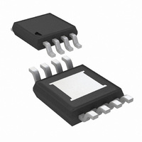
LME49726MY/NOPB National Semiconductor, LME49726MY/NOPB Datasheet - Page 3

LME49726MY/NOPB
Manufacturer Part Number
LME49726MY/NOPB
Description
IC AMP AUDIO STER AB HIFI 8MSOP
Manufacturer
National Semiconductor
Datasheet
1.LME49726MYNOPB.pdf
(22 pages)
Specifications of LME49726MY/NOPB
Amplifier Type
Audio
Number Of Circuits
2
Slew Rate
3.7 V/µs
Gain Bandwidth Product
6.25MHz
Current - Input Bias
0.2pA
Voltage - Input Offset
500µV
Current - Supply
700µA
Current - Output / Channel
350mA
Voltage - Supply, Single/dual (±)
2.5 V ~ 5.5 V, ±1.25 V ~ 2.75 V
Operating Temperature
-40°C ~ 85°C
Mounting Type
Surface Mount
Package / Case
8-MSOP Exposed Pad, 8-HMSOP, 8-eMSOP
Lead Free Status / RoHS Status
Lead free / RoHS Compliant
Output Type
-
-3db Bandwidth
-
Other names
LME49726MYTR
THD+N
GBWP
SR
t
e
e
I
V
ΔV
PSRR
ISO
I
ΔI
I
V
CMRR
1/f
A
s
N
B
OS
N
N
OS
IN-CM
VOL
OS
Absolute Maximum Ratings
2)
If Military/Aerospace specified devices are required,
please contact the National Semiconductor Sales Office/
Distributors for availability and specifications.
Electrical Characteristics (V
the circuit shown in Figure 1. V
20–20kHz, and T
Symbol
Power Supply Voltage
Storage Temperature
Input Voltage
Output Short Circuit (Note 3)
Power Dissipation
OS
CH-CH
/ΔTemp
/ΔTemp
V
S
= V
SS
Total Harmonic Distortion + Noise
Gain Bandwidth Product
Slew Rate
Settling time
Equivalent Input Noise Voltage
Equivalent Input Noise Density
Current Noise Density
Input Offset Voltage
Average Input Offset Voltage Drift vs
Temperature
Power Supply Rejection Ratio
Channel-to-Channel Isolation
Input Bias Current
Input Bias Current Drift vs
Temperature
Input Offset Current
Common-Mode Input Voltage Range
Common Mode Rejection Ratio
1/f Corner Frequency
Open-Loop Voltage Gain
-V
DD
A
= 25°C, unless otherwise specified.
Parameter
DD
(V
= 5.0V and V
SS
) – 0.7V to (V
Internally Limited
−65°C to 150°C
(Note
DD
DD
Continuous
DD
= 2.5V, V
A
A
A
A
0.1% error range
0.001% error range
f
f = 10kHz (A-weighted)
f = 1kHz (A-weighted)
f = 100Hz (A-weighted)
f = 1kHz
V
40°C
2.5 to 5.5V, V
f
V
–40°C
V
0.1V < V
V
BW
IN
= 5.0V and V
) + 0.7V
V
V
V
V
IN
CM
CM
OUT
R
R
R
R
R
R
1,
= 1kHz
= 1V step
= –1, V
= –1, V
= +1, R
= V
L
L
L
L
L
L
= 20Hz to 20kHz (A-weighted)
= V
= V
Note
= 600Ω
= 2kΩ
= 10kΩ
= 600Ω
= 2kΩ
= 10kΩ
= V
≤
6V
≤
DD/2
T
DD
DD
SS
DD
DD
T
A
OUT
OUT
/2
/2
L
A
, V
≤
/2
= 0.0V, V
– 1.6V
= 10kΩ
≤
Conditions
3
85°C
O
CM
= 3.5V
= 1.5V
85°C
= V
= 0, V
Temperature Range
Supply Voltage Range
Operating Ratings
ESD Rating (Note 4)
ESD Rating (Note 5)
Junction Temperature
Thermal Resistance
θ
DD/2
T
CM
MIN
p-p
p-p
JA
DD
, A
DD
, V
, V
(MUY-08)
= V
≤
/2
V
DD
DD
TA
= 2.5V)
= 1
DD/2
= 5V
= 2.5V
≤
, R
T
MAX
L
= 10kΩ, C
The following specifications apply for
(Note
0.00008
Typical
0.0008
0.0002
0.0008
0.0002
0.001
6.25
0.75
±0.2
±0.2
800
104
120
3.7
1.2
0.7
6.9
0.5
1.2
15
35
94
35
95
2
LOAD
6)
LME49726
(Note
= 20pF, f
V
(Note
V
1)
−40°C
Limit
DD
SS
1.25
2.25
100
5.0
2.5
85
80
IN
+0.1
2.5V
–1.6
= 1kHz, BW =
7)
≤
≤
www.national.com
T
A
V
72°C/W
≤
S
MHz (min)
V/μs (min)
mV (max)
dB (min)
dB (min)
dB (min)
(Limits)
2000V
150°C
V (min)
≤
μV
nV/
nV/
nV/
pA/
125°C
μV/°C
nA/°C
Units
(max)
200V
kHz
dB
pA
pA
5.5V
ns
μs
%
%
%
%
%
%
RMS
√
√
√
√
Hz
Hz
Hz
Hz


