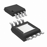
LME49726MY/NOPB National Semiconductor, LME49726MY/NOPB Datasheet - Page 9

LME49726MY/NOPB
Manufacturer Part Number
LME49726MY/NOPB
Description
IC AMP AUDIO STER AB HIFI 8MSOP
Manufacturer
National Semiconductor
Datasheet
1.LME49726MYNOPB.pdf
(22 pages)
Specifications of LME49726MY/NOPB
Amplifier Type
Audio
Number Of Circuits
2
Slew Rate
3.7 V/µs
Gain Bandwidth Product
6.25MHz
Current - Input Bias
0.2pA
Voltage - Input Offset
500µV
Current - Supply
700µA
Current - Output / Channel
350mA
Voltage - Supply, Single/dual (±)
2.5 V ~ 5.5 V, ±1.25 V ~ 2.75 V
Operating Temperature
-40°C ~ 85°C
Mounting Type
Surface Mount
Package / Case
8-MSOP Exposed Pad, 8-HMSOP, 8-eMSOP
Lead Free Status / RoHS Status
Lead free / RoHS Compliant
Output Type
-
-3db Bandwidth
-
Other names
LME49726MYTR
Application Information
DISTORTION MEASUREMENTS
The vanishingly low residual distortion produced by
LME49726 is below the capabilities of all commercially avail-
able equipment. This makes distortion measurements just
slightly more difficult than simply connecting a distortion me-
ter to the amplifier's inputs and outputs. The solution. howev-
er, is quite simple: an additional resistor. Adding this resistor
extends the resolution of the distortion measurement equip-
ment.
The LME49726's low residual is an input referred internal er-
ror. As shown in Figure 3, adding the 10Ω resistor connected
between athe amplifier's inverting and non-inverting inputs
OPERATING RATINGS AND BASIC DESIGN GUIDELINES
The LME49726 has a supply voltage range from +2.5V to
+5.5V single supply or ±1.25 to ±2.75V dual supply.
Bypassed capacitors for the supplies should be placed as
close to the amplifier as possible. This will help minimize any
inductance between the power supply and the supply pins. In
addition to a 10μF capacitor, a 0.1μF capacitor is also rec-
ommended in CMOS amplifiers.
The amplifier's inputs lead lengths should also be as short as
possible. If the op amp does not have a bypass capacitor, it
may oscillate.
BASIC AMPLIFIER CONFIGURATIONS
The LME49726 may be operated with either a single supply
or dual supplies. Figure 2 shows the typical connection for a
single supply inverting amplifier. The output voltage for a sin-
gle supply amplifier will be centered around the common-
mode voltage, V
insures the output stays above ground. Typically, the V
should be equal to V
divider circuit at this node, see
CM
. Note, the voltage applied to the V
DD
/2. This is done by putting a resistor
Figure
FIGURE 3. THD+N and IMD Distortion Test Circuit
4.
CM
CM
9
changes the amplifier's noise gain. The result is that the error
signal (distortion) is amplified by a factor of 101. Although the
amplifier's closed-loop gain is unaltered, the feedback avail-
able to correct distortion errors is reduced by 101. To ensure
minimum effects on distortion measurements, keep the value
of R1 low as shown in Figure 3.
This technique is verified by duplicating the measurements
with high closed loop gain and/or making the measurements
at high frequencies. Doing so, produces distortion compo-
nents that are within measurement equipment capabilities.
This datasheet's THD+N and IMD values were generated us-
ing the above described circuit connected to an Audio Preci-
sion System Two Cascade.
FIGURE 4. Single Supply Inverting Op Amp
300386x2
300386n3
www.national.com


