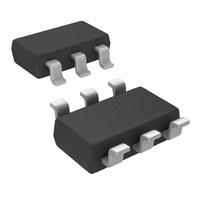
LMH6618MK/NOPB National Semiconductor, LMH6618MK/NOPB Datasheet - Page 2

LMH6618MK/NOPB
Manufacturer Part Number
LMH6618MK/NOPB
Description
IC OP AMP SGL VF RRIO TSOT23-6
Manufacturer
National Semiconductor
Series
PowerWise®r
Datasheet
1.LMH6618MKNOPB.pdf
(28 pages)
Specifications of LMH6618MK/NOPB
Amplifier Type
Voltage Feedback
Number Of Circuits
1
Output Type
Rail-to-Rail
Slew Rate
57 V/µs
Gain Bandwidth Product
65MHz
-3db Bandwidth
140MHz
Current - Input Bias
1.5µA
Voltage - Input Offset
100µV
Current - Supply
1.35mA
Current - Output / Channel
35mA
Voltage - Supply, Single/dual (±)
2.7 V ~ 11 V, ±1.35 V ~ 5.5 V
Operating Temperature
-40°C ~ 125°C
Mounting Type
Surface Mount
Package / Case
TSOT-23-6, TSOT-6
For Use With
551600083-001 - BOARD FOR SOT23 LMH6611/18
Lead Free Status / RoHS Status
Lead free / RoHS Compliant
Other names
LMH6618MK
LMH6618MK
LMH6618MKTR
LMH6618MK
LMH6618MKTR
www.national.com
Frequency Domain Response
SSBW
GBW
GBW
LSBW
Peak
0.1
dBBW
DG
DP
Time Domain Response
t
SR
t
t
Noise and Distortion Performance
SFDR
e
i
CT
Input, DC Performance
V
TCV
I
I
Symbol
n
r
s_0.1
s_0.01
B
OS
/t
n
OS
ESD Tolerance (Note 2)
Absolute Maximum Ratings
If Military/Aerospace specified devices are required,
please contact the National Semiconductor Sales Office/
Distributors for availability and specifications.
+3V Electrical Characteristics
V
Boldface Limits apply at temperature extremes. (Note 4)
f
+
Human Body Model
Machine Model
OS
= 3V, V
For input pins only
For all other pins
–3 dB Bandwidth Small Signal
Gain Bandwidth (LMH6618)
Gain Bandwidth (LMH6619)
−3 dB Bandwidth Large Signal
Peaking
0.1 dB Bandwidth
Differential Gain
Differential Phase
Rise & Fall Time
Slew Rate
0.1% Settling Time
0.01% Settling Time
Spurious Free Dynamic Range
Input Voltage Noise Density
Input Current Noise Density
Crosstalk (LMH6619)
Input Offset Voltage
Input Offset Voltage Temperature Drift (Note 5)
Input Bias Current
Input Offset Current
−
= 0V, DISABLE = 3V, V
Parameter
CM
= V
O
= V
(Note 1)
+
A
A
A
R
A
R
A
A
A
A
R
A
R
A
R
2V Step, A
2V Step, A
2V Step, A
2V Step, A
f
f
f
f = 100 kHz
f = 100 kHz
f = 5 MHz, V
V
V
V
V
/2, A
C
C
C
V
V
V
V
V
V
V
V
V
V
CM
CM
CM
CM
L
L
F
L
L
= 100 kHz, V
= 1 MHz, V
= 5 MHz, V
= 1 kΩ, V
= 1 kΩ, V
= 150Ω to V
= 150Ω to V
= 1, R
= 2, −1, R
= 10, R
= 10, R
= 1, R
= 2, R
= 1, C
= 2, V
= R
= +2, 4.43 MHz, 0.6V < V
= +2, 4.43 MHz, 0.6V < V
Unless otherwise specified, all limits are guaranteed for T
= 0.5V (pnp active)
= 2.5V (npn active)
= 0.5V (pnp active)
= 2.5V (npn active)
V
2000V
2000V
= +1 (R
G
200V
= 825Ω
OUT
L
L
L
L
F
F
V
V
V
V
= 1 kΩ, V
= 1 kΩ, V
= 150Ω, V
= 5 pF
= 2 kΩ, R
= 2 kΩ, R
= 1
= 1
= −1
= −1
IN
OUT
OUT
L
= 0.5 V
OUT
OUT
F
= 1 kΩ, V
= 2 V
+
+
2
Condition
OUT
= 0Ω), otherwise R
/2
/2
= 0.2 V
= 0.2 V
= 2 V
= 2 V
= 2 V
Supply Voltage (V
Junction Temperature (Note 3)
Supply Voltage (V
Ambient Temperature Range (Note 3)
Package Thermal Resistance (θ
Operating Ratings
PP
OUT
OUT
PP
OUT
6-Pin TSOT23
8-Pin SOIC
G
G
PP
PP
,
= 221Ω,
= 221Ω,
PP
PP
OUT
PP
= 0.2 V
= 2 V
= 2 V
, R
, R
, R
= 0.2 V
L
L
OUT
OUT
L
= 1 kΩ
= 1 kΩ
PP
PP
= 1 kΩ
PP
< 2V,
< 2V,
F
PP
= 2 kΩ for A
S
S
= V
= V
+
+
(Note 8)
– V
– V
Min
55
55
36
−
−
)
)
V
≠
JA
(Note 1)
+1, R
(Note 7)
)
−1.4
+1.0
0.01
Typ
120
120
100
1.5
0.1
0.1
0.1
0.8
56
71
63
13
13
15
36
46
90
61
47
10
80
1
L
= 1 kΩ || 5 pF.
J
= +25°C,
(Note 8)
−40°C to +125°C
±0.27
±0.6
±1.0
−2.6
+1.8
Max
2.7V to 11V
150°C max
231°C/W
160°C/W
nV/
pA/
μV/°C
Units
MHz
MHz
MHz
MHz
MHz
V/μs
deg
dBc
mV
dB
dB
μA
μA
ns
ns
12V
%


