LF442CN/NOPB National Semiconductor, LF442CN/NOPB Datasheet
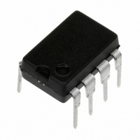
IC OP AMP DUAL LO PWR JFET 8-DIP

LF442CN/NOPB

Manufacturer Part Number
LF442CN/NOPB
Description
IC OP AMP DUAL LO PWR JFET 8-DIP
Manufacturer
National Semiconductor
Series
BI-FET II™r
Datasheets

Specifications of LF442CN/NOPB

Amplifier Type
J-FET
Number Of Circuits
2
Slew Rate
1 V/µs
Gain Bandwidth Product
1MHz
Current - Input Bias
10pA
Voltage - Input Offset
1000µV
Current - Supply
400µA
Voltage - Supply, Single/dual (±)
10 V ~ 36 V, ±5 V ~ 18 V
Operating Temperature
0°C ~ 70°C
Mounting Type
Through Hole
Package / Case
8-DIP (0.300", 7.62mm)
Bandwidth
1 MHz
Channel Separation
-120
Common Mode Rejection Ratio
95
Current, Input Bias
10 pA
Current, Input Offset
5 pA
Current, Output
6.8 mA
Current, Supply
400 μA
Impedance, Thermal
152 °C/W
Number Of Amplifiers
Dual
Package Type
MDIP-8
Resistance, Input
10^12 Ohms
Temperature, Operating, Range
0 to +70 °C
Voltage, Gain
200 V/mV
Voltage, Input
6 to 44 V
Voltage, Noise
35 nV/sqrt Hz
Voltage, Offset
1 mV
Voltage, Output, High
13 V
Voltage, Output, Low
-13 V
Voltage, Supply
±15 V
Lead Free Status / RoHS Status
Lead free / RoHS Compliant
Output Type
-
Current - Output / Channel
-
-3db Bandwidth
-
Lead Free Status / Rohs Status
RoHS Compliant part Electrostatic Device
Other names
*LF442CN
*LF442CN/NOPB
LF442
LF442CN
© 2004 National Semiconductor Corporation
LF442
Dual Low Power JFET Input Operational Amplifier
General Description
The LF442 dual low power operational amplifiers provide
many of the same AC characteristics as the industry stan-
dard LM1458 while greatly improving the DC characteristics
of the LM1458. The amplifiers have the same bandwidth,
slew rate, and gain (10 kΩ load) as the LM1458 and only
draw one tenth the supply current of the LM1458. In addition
the well matched high voltage JFET input devices of the
LF442 reduce the input bias and offset currents by a factor of
10,000 over the LM1458. A combination of careful layout
design and internal trimming guarantees very low input offset
voltage and voltage drift. The LF442 also has a very low
equivalent input noise voltage for a low power amplifier.
The LF442 is pin compatible with the LM1458 allowing an
immediate 10 times reduction in power drain in many appli-
cations. The LF442 should be used where low power dissi-
pation and good electrical characteristics are the major con-
siderations.
Typical Connection
Ordering Information
LF442XYZ
X indicates electrical grade
Y indicates temperature range
Z indicates package type
BI-FET II
“M” for military
“C” for commercial
“H” or “N”
is a trademark of National Semiconductor Corporation.
DS009155
00915501
Features
n 1/10 supply current of a LM1458:
n Low input bias current: 50 pA (max)
n Low input offset voltage: 1 mV (max)
n Low input offset voltage drift: 10 µV/˚C (max)
n High gain bandwidth: 1 MHz
n High slew rate: 1 V/µs
n Low noise voltage for low power:
n Low input noise current:
n High input impedance: 10
n High gain V
Connection Diagrams
Pin 4 connected to case
Order Number LF442AMH or LF442MH/883
Order Number LF442ACN or LF442CN
See NS Package Number H08A
See NS Package Number N08E
O
=
Dual-In-Line Package
±
Metal Can Package
10V, R
Top View
Top View
L
= 10k: 50k (min)
12
400 µA (max)
00915502
00915504

Related parts for LF442CN/NOPB

LF442CN/NOPB Summary of contents

Page 1

... Z indicates package type “H” or “N” BI-FET II ™ trademark of National Semiconductor Corporation. © 2004 National Semiconductor Corporation Features n 1/10 supply current of a LM1458: n Low input bias current (max) n Low input offset voltage (max) n Low input offset voltage drift: 10 µ ...

Page 2

... Absolute Maximum Ratings If Military/Aerospace specified devices are required, please contact the National Semiconductor Sales Office/ Distributors for availability and specifications. LF442A ± Supply Voltage 22V ± Differential Input Voltage 38V ± Input Voltage Range 19V (Note 2) Output Short Circuit Continuous Duration (Note 3) ...

Page 3

AC Electrical Characteristics Symbol Parameter Amplifier to Amplifier Coupling SR Slew Rate GBW Gain-Bandwidth Product e Equivalent Input Noise n Voltage i Equivalent Input Noise n Current Note 1: “Absolute Maximum Ratings” indicate limits beyond which damage to the device ...

Page 4

... BANNED SUBSTANCE COMPLIANCE National Semiconductor certifies that the products and packing materials meet the provisions of the Customer Products Stewardship Specification (CSP-9-111C2) and the Banned Substances and Materials of Interest Specification (CSP-9-111S2) and contain no ‘‘Banned Substances’’ as defined in CSP-9-111S2. ...

Related keywords