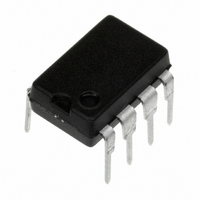
LF442CN/NOPB National Semiconductor, LF442CN/NOPB Datasheet

LF442CN/NOPB
Specifications of LF442CN/NOPB
*LF442CN/NOPB
LF442
LF442CN
Related parts for LF442CN/NOPB
LF442CN/NOPB Summary of contents
Page 1
... Z indicates package type “H” or “N” BI-FET II ™ trademark of National Semiconductor Corporation. © 2004 National Semiconductor Corporation Features n 1/10 supply current of a LM1458: n Low input bias current (max) n Low input offset voltage (max) n Low input offset voltage drift: 10 µ ...
Page 2
... Absolute Maximum Ratings If Military/Aerospace specified devices are required, please contact the National Semiconductor Sales Office/ Distributors for availability and specifications. LF442A Supply Voltage Differential Input Voltage Input Voltage Range (Note 2) Output Short Circuit Continuous Duration (Note 3) H Package T max 150˚C ...
Page 3
AC Electrical Characteristics Symbol Parameter Amplifier to Amplifier Coupling SR Slew Rate GBW Gain-Bandwidth Product e Equivalent Input Noise n Voltage i Equivalent Input Noise n Current Note 1: “Absolute Maximum Ratings” indicate limits beyond which damage to the device ...
Page 4
Typical Performance Characteristics Input Bias Current Supply Current Negative Common-Mode Input Voltage Limit www.national.com 00915517 Positive Common-Mode 00915519 Positive Current Limit 00915521 4 Input Bias Current 00915518 Input Voltage Limit 00915520 00915522 ...
Page 5
Typical Performance Characteristics Negative Current Limit Output Voltage Swing Bode Plot (Continued) Output Voltage Swing 00915523 00915525 00915527 5 00915524 Gain Bandwidth 00915526 Slew Rate 00915528 www.national.com ...
Page 6
Typical Performance Characteristics Distortion vs Frequency Open Loop Frequency Response Power Supply Rejection Ratio www.national.com (Continued) Undistorted Output Voltage 00915529 Common-Mode Rejection 00915531 Equivalent Input Noise 00915533 6 Swing 00915530 Ratio 00915532 Voltage 00915534 ...
Page 7
Typical Performance Characteristics Open Loop Voltage Gain Inverter Settling Time (Continued) 00915535 00915537 7 Output Impedance 00915536 www.national.com ...
Page 8
Pulse Response kΩ Small Signal Inverting Small Signal Non-Inverting www.national.com = 00915507 Large Signal Non-Inverting 00915508 8 Large Signal Inverting 00915509 00915510 ...
Page 9
Application Hints This device is a dual low power op amp with internally trimmed input offset voltages and JFET input devices (BI- FET II). These JFETs have large reverse breakdown volt- ages from gate to source and drain eliminating the ...
Page 10
Typical Applications Trim 1M pot for 1 kHz full-scale output 15 mW power drain No integrator reset FET required Mount D1 and D2 in close proximity 1% linearity to 1 kHz • 75˚C control • A1’s output represents ...
Page 11
Typical Applications (Continued Tel Labs type Q81 T Trim 5k for 10 µA through the 5k–120k combination *1% film resistor Q1, Q2, Q3 are included on LM389 amplifier chip which is temperature-stabilized by the LM389 and Q2-Q3, which ...
Page 12
Detailed Schematic www.national.com 1/2 Dual 00915516 12 ...
Page 13
Physical Dimensions inches (millimeters) unless otherwise noted TO-5 Metal Can Package (H) Order Number LF442AMH or LF442MH/883 NS Package Number H08A 13 www.national.com ...
Page 14
... BANNED SUBSTANCE COMPLIANCE National Semiconductor certifies that the products and packing materials meet the provisions of the Customer Products Stewardship Specification (CSP-9-111C2) and the Banned Substances and Materials of Interest Specification (CSP-9-111S2) and contain no ‘‘Banned Substances’’ as defined in CSP-9-111S2. ...


