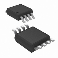
LMH6504MM/NOPB National Semiconductor, LMH6504MM/NOPB Datasheet - Page 2

LMH6504MM/NOPB
Manufacturer Part Number
LMH6504MM/NOPB
Description
IC AMP VAR GAIN LOW POWER 8MSOP
Manufacturer
National Semiconductor
Series
LMH®r
Type
Variable Gain Amplifierr
Datasheet
1.LMH6504MMNOPB.pdf
(19 pages)
Specifications of LMH6504MM/NOPB
Amplifier Type
Variable Gain
Number Of Circuits
1
Slew Rate
1500 V/µs
-3db Bandwidth
150MHz
Current - Input Bias
1.4µA
Current - Supply
11mA
Current - Output / Channel
80mA
Voltage - Supply, Single/dual (±)
7 V ~ 12 V, ±3.5 V ~ 6 V
Operating Temperature
-40°C ~ 85°C
Mounting Type
Surface Mount
Package / Case
8-MSOP, Micro8™, 8-uMAX, 8-uSOP,
Number Of Channels
1
Number Of Elements
1
Power Supply Requirement
Dual
Input Resistance
7MOhm
Input Bias Current
3.5uA
Single Supply Voltage (typ)
Not RequiredV
Dual Supply Voltage (typ)
±5V
Power Supply Rejection Ratio
65dB
Rail/rail I/o Type
No
Single Supply Voltage (min)
Not RequiredV
Single Supply Voltage (max)
Not RequiredV
Dual Supply Voltage (min)
±3.5V
Dual Supply Voltage (max)
±6V
Operating Temp Range
-40C to 85C
Operating Temperature Classification
Industrial
Mounting
Surface Mount
Pin Count
8
Package Type
MSOP
Lead Free Status / RoHS Status
Lead free / RoHS Compliant
Output Type
-
Gain Bandwidth Product
-
Voltage - Input Offset
-
Lead Free Status / Rohs Status
Compliant
Other names
LMH6504MM
LMH6504MMTR
LMH6504MMTR
Available stocks
Company
Part Number
Manufacturer
Quantity
Price
www.national.com
Frequency Domain Response
BW
GF
Att Range Flat Band (Relative to Max Gain)
BW
Control
CT (dB)
GR
Time Domain Response
t
OS %
SR
Distortion & Noise Performance
HD2
HD3
THD
En tot
I
DG
DP
r
N
Symbol
, t
Absolute Maximum Ratings
If Military/Aerospace specified devices are required,
please contact the National Semiconductor Sales Office/
Distributors for availability and specifications.
Electrical Characteristics
Unless otherwise specified, all limits guaranteed for T
±
ESD Tolerance (Note 4):
Input Current
Output Current
Supply Voltages (V
Voltage at Input/ Output pins
Storage Temperature Range
f
0.1V, R
Human Body Model
Machine Model
L
-3dB Bandwidth
Gain Flatness
Attenuation Range (Note 13)
Gain control Bandwidth
Feed-through
Gain Adjustment Range
Rise and Fall Time
Overshoot
Slew Rate (Note 5)
2
3
Total Harmonic Distortion
Total Equivalent Input Noise
Input Noise Current
Differential Gain
Differential Phase
= 100Ω, V
nd
rd
Harmonic Distortion
Harmonic Distortion
+
G
- V
Parameter
= +2V. Boldface limits apply at the temperature extremes.
−
)
V
+
120 mA (Note 3)
(Note 2)
+0.8V, V
−65˚C to 150˚C
(Note 1)
V
V
V
0.9V ≤ V
±
±
V
V
(Output/Input)
f
f
0.5V Step
4V Step, Non Inverting
4V Step, Inverting
2V
f
f
f = 4.43 MHz, R
OUT
OUT
OUT
G
G
<
<
>
>
0.2 dB Flatness, f
0.1 dB Flatness, f
PP
±
−
= 1V (Note 12)
= 0V, 30 MHz
10 MHz
30 MHz
1 MHz, R
1 MHz
10 mA
1000V
−0.8V
, 20 MHz
12.6V
100V
<
<
<
A
= 25˚C, V
1 V
4 V
1 V
G
Conditions
≤ 2V,
PP
PP
PP
SOURCE
, A
2
L
VMAX
±
S
= 100Ω
0.2 dB
Operating Ratings
=
<
<
Junction Temperature
Soldering Information:
Supply Voltages (V
Temperature Range (Note 15)
Thermal Resistance:
= 50Ω
±
Infrared or Convection (20 sec)
Wave Soldering (10 sec)
30 MHz
30 MHz
8 -Pin SOIC
8-Pin MSOP
= 100
5V, A
VMAX
(Note 6)
= 9.7 V/V, R
Min
+
- V
−
)
(Note 6)
F
1500
0.45
0.13
Typ
150
150
−53
800
−47
–55
−45
9.5
2.1
4.4
2.6
58
40
26
80
73
20
= 1 kΩ, R
(θ
(Note 1)
60
65
JC
)
G
(Note 6)
= 100Ω, V
Max
−40˚C to +85˚C
(θ
165
235
7V to 12V
JA
)
150˚C
235˚C
260˚C
nV/
pA/
IN
Units
MHz
MHz
MHz
V/µs
dBc
deg
=
dB
dB
dB
ns
%
%


