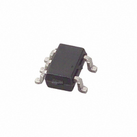
MAX4291EXK+T Maxim Integrated Products, MAX4291EXK+T Datasheet - Page 10

MAX4291EXK+T
Manufacturer Part Number
MAX4291EXK+T
Description
IC OP AMP R-R I/O SC70-5
Manufacturer
Maxim Integrated Products
Datasheet
1.MAX4291EUKT.pdf
(18 pages)
Specifications of MAX4291EXK+T
Amplifier Type
General Purpose
Number Of Circuits
1
Output Type
Rail-to-Rail
Slew Rate
0.2 V/µs
Gain Bandwidth Product
500kHz
Current - Input Bias
15nA
Voltage - Input Offset
400µV
Current - Supply
100µA
Current - Output / Channel
20mA
Voltage - Supply, Single/dual (±)
1.8 V ~ 5.5 V, ±0.9 V ~ 2.75 V
Operating Temperature
-40°C ~ 85°C
Mounting Type
Surface Mount
Package / Case
SC-70-5, SC-88A, SOT-323-5, SOT-353, 5-TSSOP
Number Of Channels
1
Voltage Gain Db
130 dB
Common Mode Rejection Ratio (min)
50 dB
Input Offset Voltage
2.5 mV
Operating Supply Voltage
3 V, 5 V
Maximum Power Dissipation
200 mW
Maximum Operating Temperature
+ 85 C
Mounting Style
SMD/SMT
Maximum Dual Supply Voltage
+/- 2.75 V
Minimum Operating Temperature
- 40 C
Lead Free Status / RoHS Status
Lead free / RoHS Compliant
-3db Bandwidth
-
Lead Free Status / Rohs Status
Details
Other names
MAX4291EXK+T
MAX4291EXK+TTR
MAX4291EXK+TTR
variety of typical battery types showing voltage when
fresh, voltage at end-of-life, capacity, and approximate
operating time from a MAX4291 (assuming nominal
conditions).
Although the amplifiers are fully guaranteed over tem-
perature for operation down to a 1.8V single supply,
even lower voltage operation is possible in practice.
Figures 4 and 5 show the offset voltage and supply cur-
rent as a function of supply voltage and temperature.
The MAX4291/MAX4292/MAX4294 are fully guaranteed
over temperature and supply voltage range to drive a
maximum resistive load of 2k
heavier loads can be driven in many applications. The
rail-to-rail output stage of the amplifier can be modeled
Ultra-Small, 1.8V, µPower,
Rail-to-Rail I/O Op Amps
Figure 4. Offset Voltage vs. Supply Voltage
Figure 5. Supply Current per Amplifier vs. Supply Voltage
10
______________________________________________________________________________________
-450
-500
-550
-600
-650
-700
140
120
100
80
60
40
20
0
OFFSET VOLTAGE vs. SUPPLY VOLTAGE
0
0
0.5
SUPPLY CURRENT PER AMPLIFIER
0.5
T
A
1.0 1.5
1.0
= +85 C
vs. SUPPLY VOLTAGE
1.5
SUPPLY VOLTAGE (V)
SUPPLY VOLTAGE (V)
2.0
2.0 2.5 3.0
MAX4291
Load-Driving Capability
T
2.5
T
A
A
= +25 C
= +85 C
T
3.0
A
= +25 C
3.5 4.0 4.5 5.0 5.5
3.5
V
T
4.0
CM
A
to V
= -40 C
T
A
= V
4.5 5.0
= -40 C
CC
CC
/2
5.5
/2, although
as a current source when driving the load toward V
and as a current sink when driving the load toward V
The limit of this current source/sink varies with supply
voltage, ambient temperature, and lot-to-lot variations
of the units.
Figures 6a and 6b show the typical current source and
sink capabilities of the MAX4291/MAX4292/MAX4294
family as a function of supply voltage and ambient tem-
perature. The contours on the graph depict the output
current value, based on driving the output voltage to
within 50mV, 100mV, and 200mV of either power-sup-
ply rail.
For example, a MAX4291 running from a single 1.8V
supply, operating at T
Figure 6a. Output Source Current vs. Temperature
Figure 6b. Output Sink Current vs. Temperature
30
25
20
15
10
18
16
14
12
10
5
0
8
6
4
2
0
-55
-55
V
V
V
V
V
V
V
V
CC
OH
CC
OL
-40
-40
CC
OH
CC
OL
= 100mV
= 5.5V
= 50mV V
= 5.5V
-25
-25
OUTPUT SOURCE CURRENT
= 5.5V
= 200mV
= 200mV
= 5.5V
OUTPUT SINK CURRENT
-10
-10
vs. TEMPERATURE
vs. TEMPERATURE
TEMPERATURE (°C)
TEMPERATURE (°C)
A
V
5 20 35
5 20 35
CC
OH
V
V
V
V
V
V
= +25°C can source 3.5mA to
CC
OL
CC
OH
CC
OL
= 1.8V
= 100mV
= 100mV
= 1.8V
= 1.8V
= 200mV
= 50mV
= 5.5V
50
50
V
OH
V
65
65
OL
V
V
= V
V
V
V
V
V
V
CC
OH
= V
CC
OH
CC
OL
CC
OL
80
80
CC
= 1.8V
= 50mV
= 5.5V
= 100mV
OUT
= 200mV
= 50mV
= 1.8V
= 1.8V
- V
95
95
- V
OUT
110
110
EE
125
125
CC
EE
,
.


