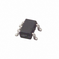
MAX4291EXK+T Maxim Integrated Products, MAX4291EXK+T Datasheet - Page 2

MAX4291EXK+T
Manufacturer Part Number
MAX4291EXK+T
Description
IC OP AMP R-R I/O SC70-5
Manufacturer
Maxim Integrated Products
Datasheet
1.MAX4291EUKT.pdf
(18 pages)
Specifications of MAX4291EXK+T
Amplifier Type
General Purpose
Number Of Circuits
1
Output Type
Rail-to-Rail
Slew Rate
0.2 V/µs
Gain Bandwidth Product
500kHz
Current - Input Bias
15nA
Voltage - Input Offset
400µV
Current - Supply
100µA
Current - Output / Channel
20mA
Voltage - Supply, Single/dual (±)
1.8 V ~ 5.5 V, ±0.9 V ~ 2.75 V
Operating Temperature
-40°C ~ 85°C
Mounting Type
Surface Mount
Package / Case
SC-70-5, SC-88A, SOT-323-5, SOT-353, 5-TSSOP
Number Of Channels
1
Voltage Gain Db
130 dB
Common Mode Rejection Ratio (min)
50 dB
Input Offset Voltage
2.5 mV
Operating Supply Voltage
3 V, 5 V
Maximum Power Dissipation
200 mW
Maximum Operating Temperature
+ 85 C
Mounting Style
SMD/SMT
Maximum Dual Supply Voltage
+/- 2.75 V
Minimum Operating Temperature
- 40 C
Lead Free Status / RoHS Status
Lead free / RoHS Compliant
-3db Bandwidth
-
Lead Free Status / Rohs Status
Details
Other names
MAX4291EXK+T
MAX4291EXK+TTR
MAX4291EXK+TTR
ABSOLUTE MAXIMUM RATINGS
Supply Voltage (V
All Other Pins ...................................(V
Current into IN_+, IN_- .....................................................
Output Short-Circuit Duration.....................................Continuous
Continuous Power Dissipation (T
Stresses beyond those listed under “Absolute Maximum Ratings” may cause permanent damage to the device. These are stress ratings only, and functional
operation of the device at these or any other conditions beyond those indicated in the operational sections of the specifications is not implied. Exposure to
absolute maximum rating conditions for extended periods may affect device reliability.
Ultra-Small, 1.8V, µPower,
Rail-to-Rail I/O Op Amps
ELECTRICAL CHARACTERISTICS
(V
(Note 1)
2
Supply Voltage Range
Quiescent Supply Current
(Per Amplifier)
Input Offset Voltage
Input Bias Current
Input Offset Current
Differential Input Resistance
Input Common-Mode Voltage
Range
Common-Mode Rejection Ratio
Common-Mode Rejection Ratio
Power-Supply Rejection Ratio
CC
5-Pin SC70 (derate 2.5mW/°C above +70°C) ................200mW
5-Pin SOT23 (derate 7.1mW/°C above +70°C)................571mW
8-Bump UCSP (derate 4.7mW/°C above +70°C) ...........379mW
_______________________________________________________________________________________
= 1.8V to 5.5V, V
PARAMETER
CC
to V
EE
EE)
= V
....................................................6V
CM
A
= +70°C)
= 0, V
SYMBOL
CMRR
PSRR
CC
V
V
V
I
R
OS
I
I
OS
CM
CC
B
IN
Q
+ 0.3V) to (V
OUT
= V
Inferred from PSRR test
V
V
MAX4291
MAX4292/MAX4294
V
V
|V
Inferred from CMRR test
Tested for
0
1.8V;
V
Tested for
0
5.0V,
V
CC
CC
CC
CC
CC
CC
IN+
CC
V
V
= 1.8V
= 5.0V
= 5.0V, 0
= 5.0V, 0
= 1.8V
= 5.0V
CM
CM
- V
EE
/2, R
±
IN-
- 0.3V)
25mA
| < 10mV
L
= 100k
CONDITIONS
V
V
MAX4291
MAX4292/MAX4294
MAX4291
MAX4292/MAX4294
CM
CM
Operating Temperature Range............................-40°C to +85°C
Junction Temperature ......................................................+150°C
Storage Temperature Range .............................-65°C to +150°C
Lead Temperature (soldering, 10s) .................................+300°C
5.0V
5.0V
connected to V
8-Pin µMAX (derate 4.10mW/°C above +70°C)..............330mW
8-Pin SO (derate 5.88mW/°C above +70°C) ..................471mW
14-Pin SO (derate 8.33mW/°C above +70°C) ................667mW
14-Pin TSSOP (derate 6.3mW/°C above +70°C) ............500mW
CC
/2, T
A
= +25°C, unless otherwise noted.)
MIN
1.8
50
57
60
66
77
0
±400
±200
TYP
0.75
±15
100
100
100
±1
80
80
90
90
±2500
±1200
MAX
±60
V
210
255
5.5
±7
CC
UNITS
M
dB
dB
dB
µA
µV
nA
nA
V
V


