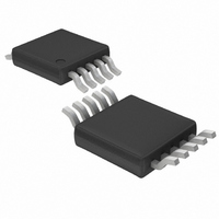
LT1995IMS Linear Technology, LT1995IMS Datasheet - Page 16

LT1995IMS
Manufacturer Part Number
LT1995IMS
Description
IC AMP GAIN SELECT 10MSOP
Manufacturer
Linear Technology
Datasheet
1.LT1995CMSPBF.pdf
(20 pages)
Specifications of LT1995IMS
Amplifier Type
Programmable Gain
Number Of Circuits
1
Slew Rate
1000 V/µs
-3db Bandwidth
32MHz
Voltage - Input Offset
500µV
Current - Supply
7.1mA
Current - Output / Channel
120mA
Voltage - Supply, Single/dual (±)
5 V ~ 30 V, ±2.5 V ~ 15 V
Operating Temperature
-40°C ~ 85°C
Mounting Type
Surface Mount
Package / Case
10-MSOP, Micro10™, 10-uMAX, 10-uSOP
Lead Free Status / RoHS Status
Contains lead / RoHS non-compliant
Output Type
-
Gain Bandwidth Product
-
Current - Input Bias
-
Available stocks
Company
Part Number
Manufacturer
Quantity
Price
Part Number:
LT1995IMS#PBF
Manufacturer:
LINEAR/凌特
Quantity:
20 000
Part Number:
LT1995IMS#TRPBF
Manufacturer:
LINEAR/凌特
Quantity:
20 000
APPLICATIO S I FOR ATIO
LT1995
Using the LT1995 as an AC-coupled inverting gain stage,
the REF pin and the relevant P inputs may all be driven from
a V
establishing the quiescent voltage on the input and output
pins. The V
current (I
(0.6µA typically), so a high V
will cause the quiescent level of the amplifier output to
deviate from the intended V
16
BIAS
V
IN
*CONFIGURE M INPUTS FOR DESIRED G PARAMETER; REFER TO FIGURE 2 FOR CONNECTIONS. ANY M
source as depicted in the example of Figure 6, thus
C
INPUTS SHOWN GROUNDED IN FIGURE 2 SHOULD INSTEAD BE CAPACITIVELY COUPLED TO GROUND
V
V
*
IN
B
IN
IN
Figure 5. AC-Coupled Difference Amplifier
General Configuation (G = 5 Example)
) of the noninverting input of the internal op amp
–
+
BIAS
V
10
BIAS
8
9
1
2
3
C
C
IN
IN
M4
M2
M1
P1
P2
P4
signal will only have to source the bias
Figure 7. AC-Coupled Noninverting Amplifier Input Attenuation Configurations (Supply Splitting)
LT1995
U
A = 0.750
10
8
9
1
2
3
4
+V
M4
M2
M1
P1
P2
P4
7
REF
5
U
LT1995
BIAS
4
+V
BIAS
7
6
REF
C
level by I
OUT
5
1995 F05
source impedance (R
W
V
OUT
6
C
V
OUT
IN
B
• R
C
V
*
IN
S
OUT
U
.
10
8
9
1
2
3
M4
M2
M1
P1
P2
P4
S
LT1995
)
A = 0.667
4
+V
7
REF
In operation as a noninverting gain stage, the P and REF
inputs may be configured as a “supply splitter,” thereby
providing a convenient mid-supply operating point. Fig-
ure 7 illustrates the three attenuation configurations that
generate 50% mid-supply biasing levels with no external
components aside from the desired coupling capacitors.
As with the DC-coupled input attenuation ratios, A, a
compound output function including the feedback gain
parameter G is given by:
5
V
OUT
6
C
V
Figure 6. AC-Coupled Inverting Gain Amplifier
General Configuration (G = 5 Example)
= A • G • V
OUT
IN
–
V
BIAS
V
OUT
C
IN
V
IN
IN
10
8
9
1
2
3
M4
M2
M1
P1
P2
P4
C
*
IN
LT1995
10
8
9
1
2
3
4
+V
M4
M2
M1
P1
P2
P4
7
REF
LT1995
5
1995 F06
A = 0.500
4
+V
7
REF
6
5
1995 F07
C
OUT
6
V
C
OUT
OUT
V
OUT
1995fb


