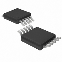
LT1995IMS Linear Technology, LT1995IMS Datasheet - Page 18

LT1995IMS
Manufacturer Part Number
LT1995IMS
Description
IC AMP GAIN SELECT 10MSOP
Manufacturer
Linear Technology
Datasheet
1.LT1995CMSPBF.pdf
(20 pages)
Specifications of LT1995IMS
Amplifier Type
Programmable Gain
Number Of Circuits
1
Slew Rate
1000 V/µs
-3db Bandwidth
32MHz
Voltage - Input Offset
500µV
Current - Supply
7.1mA
Current - Output / Channel
120mA
Voltage - Supply, Single/dual (±)
5 V ~ 30 V, ±2.5 V ~ 15 V
Operating Temperature
-40°C ~ 85°C
Mounting Type
Surface Mount
Package / Case
10-MSOP, Micro10™, 10-uMAX, 10-uSOP
Lead Free Status / RoHS Status
Contains lead / RoHS non-compliant
Output Type
-
Gain Bandwidth Product
-
Current - Input Bias
-
Available stocks
Company
Part Number
Manufacturer
Quantity
Price
Part Number:
LT1995IMS#PBF
Manufacturer:
LINEAR/凌特
Quantity:
20 000
Part Number:
LT1995IMS#TRPBF
Manufacturer:
LINEAR/凌特
Quantity:
20 000
APPLICATIO S I FOR ATIO
LT1995
and power dissipation (P
layout:
For example, in order to maintain a maximum junction
temperature of 150°C at 85°C ambient in an MS10 pack-
age, the power must be limited to 0.4W. It is important to
note that when operating at ±15V supplies, the quiescent
current alone will typically account for 0.24W, so careful
thermal management may be required if high load cur-
rents and high supply voltages are involved. By additional
copper area contact to the supply pins or effective thermal
coupling to extended ground plane(s), the thermal imped-
ance can be reduced to 130°C/W in the MS10 package. A
substantial reduction in thermal impedance of the DD10
package down to about 50°C/W can be achieved by
connecting the Exposed Pad on the bottom of the package
to a large PC board metal area which is either open-
circuited or connected to V
18
T
J
= T
A
Figure 9. Optional Frequency Compensation
Network for (1 ≤ G ≤ 2)
V
+ (P
IN
CONFIGURATION EXAMPLE:
G = 1.14
D
• θ
10
8
9
1
2
3
U
JA
M4
M2
M1
P1
P2
P4
)
LT1995
–V
D
U
4
) as follows for a nominal PCB
+V
S
7
REF
–
.
5
W
6
47Ω
10nF
1995 F09
V
OUT
U
Frequency Compensation
The LT1995 comfortably drives heavy resistive loads such
as back-terminated cables and provides nicely damped
responses for all gain configurations when doing so.
Small capacitances are included in the on-chip resistor
network to optimize bandwidth in the basic difference gain
configurations of Figure 1. For the noninverting configura-
tions of Figure 2, where the gain parameter G is 2 or less,
significant overshoot can occur when driving light loads.
For these low gain cases, providing an RC output network
as shown in Figure 9 to create an artificial load at high
frequency will assure good damping behavior.
Figure 10. Step Response of Circuit in Figure 9
1995fb


