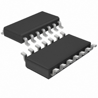
LT1259IS Linear Technology, LT1259IS Datasheet - Page 7

LT1259IS
Manufacturer Part Number
LT1259IS
Description
IC AMP DUAL CURR FDBK SD 14SOIC
Manufacturer
Linear Technology
Datasheet
1.LT1259CSPBF.pdf
(12 pages)
Specifications of LT1259IS
Amplifier Type
Current Feedback
Number Of Circuits
2
Slew Rate
1600 V/µs
-3db Bandwidth
130MHz
Current - Input Bias
20µA
Voltage - Input Offset
2000µV
Current - Supply
5mA
Current - Output / Channel
60mA
Voltage - Supply, Single/dual (±)
4 V ~ 30 V, ±2 V ~ 15 V
Operating Temperature
-40°C ~ 85°C
Mounting Type
Surface Mount
Package / Case
14-SOIC (3.9mm Width), 14-SOL
Lead Free Status / RoHS Status
Contains lead / RoHS non-compliant
Output Type
-
Gain Bandwidth Product
-
Available stocks
Company
Part Number
Manufacturer
Quantity
Price
Part Number:
LT1259IS
Manufacturer:
LINEAR/凌特
Quantity:
20 000
Part Number:
LT1259IS#PBF
Manufacturer:
LINEAR/凌特
Quantity:
20 000
Part Number:
LT1259IS#TRPBF
Manufacturer:
LINEAR/凌特
Quantity:
20 000
SI PLIFIED SCHE ATIC
APPLICATIO S I FOR ATIO
Feedback Resistor Selection
The small-signal bandwidth of the LT1259/ LT1260 are set
by the external feedback resistors and the internal junction
capacitors. As a result, the bandwidth is a function of the
supply voltage, the value of the feedback resistor, the
closed-loop gain and the load resistor. The LT1259/LT1260
have been optimized for 5V supply operation and have a
– 3dB bandwidth of 90MHz. See resistor selection guide in
Typical AC Performance table.
Capacitance on the Inverting Input
Current feedback amplifiers require resistive feedback
from the output to the inverting input for stable operation.
Take care to minimize the stray capacitance between the
output and the inverting input. Capacitance on the invert-
ing input to ground will cause peaking in the frequency
response (and overshoot in the transient response). See
the section on Demo Board Information.
Capacitive Loads
The LT1259/LT1260 can drive capacitive loads directly
when the proper value of feedback resistor is used. The
graph of Maximum Capacitive Load vs Feedback Resistor
should be used to select the appropriate value. The value
shown is for 5dB peaking when driving a 150 load at a
gain of 2. This is a worst case condition. The amplifier is
W
U
EN
U
W
W
+IN
, each amplifier
U
–IN
more stable at higher gains. Alternatively, a small resistor
(10 to 20 ) can be put in series with the output to isolate
the capacitive load from the amplifier output. This has the
advantage that the amplifier bandwidth is only reduced
when the capacitive load is present. The disadvantage is
that the gain is a function of the load resistance.
Power Supplies
The LT1259/LT1260 will operate from single or split
supplies from 2V (4V total) to 15V (30V total). It is not
necessary to use equal value split supplies, however the
offset voltage and inverting input bias current will change.
The offset voltage changes about 500 V per volt of
supply mismatch. The inverting bias current can change
as much as 5 A per volt of supply mismatch though
typically, the change is about 0.1 A per volt.
Slew Rate
The slew rate of a current feedback amplifier is not
independent of the amplifier gain configuration the way
slew rate is in a traditional op amp. This is because both the
input stage and the output stage have slew rate limitations.
In the inverting mode, and for higher gains in the nonin-
verting mode, the signal amplitude between the input pins
is small and the overall slew rate is that of the output stage.
For gains less than ten in the noninverting mode, the
overall slew rate is limited by the input stage.
LT1259/60 • SS
LT1259/LT1260
OUT
V
V
+
–
7


