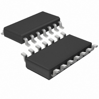
LT1259IS Linear Technology, LT1259IS Datasheet - Page 8

LT1259IS
Manufacturer Part Number
LT1259IS
Description
IC AMP DUAL CURR FDBK SD 14SOIC
Manufacturer
Linear Technology
Datasheet
1.LT1259CSPBF.pdf
(12 pages)
Specifications of LT1259IS
Amplifier Type
Current Feedback
Number Of Circuits
2
Slew Rate
1600 V/µs
-3db Bandwidth
130MHz
Current - Input Bias
20µA
Voltage - Input Offset
2000µV
Current - Supply
5mA
Current - Output / Channel
60mA
Voltage - Supply, Single/dual (±)
4 V ~ 30 V, ±2 V ~ 15 V
Operating Temperature
-40°C ~ 85°C
Mounting Type
Surface Mount
Package / Case
14-SOIC (3.9mm Width), 14-SOL
Lead Free Status / RoHS Status
Contains lead / RoHS non-compliant
Output Type
-
Gain Bandwidth Product
-
Available stocks
Company
Part Number
Manufacturer
Quantity
Price
Part Number:
LT1259IS
Manufacturer:
LINEAR/凌特
Quantity:
20 000
Part Number:
LT1259IS#PBF
Manufacturer:
LINEAR/凌特
Quantity:
20 000
Part Number:
LT1259IS#TRPBF
Manufacturer:
LINEAR/凌特
Quantity:
20 000
APPLICATIO S I FOR ATIO
LT1259/LT1260
The input slew rate of the LT1259/LT1260 is approxi-
mately 270V/ s and is set by internal currents and capaci-
tances. The output slew rate is set by the value of the
feedback resistors and internal capacitances. At a gain of
10 with at 1k feedback resistor and 15V supplies, the
output slew rate is typically 1600V/ s. Larger feedback
resistors will reduce the slew rate as will lower supply
voltages, similar to the way the bandwidth is reduced.
The graph of Maximum Undistorted Output vs Frequency
relates the slew rate limitations to sinusoidal input for
various gains.
Enable/Disable
The LT1259/LT1260 amplifiers have a unique high imped-
ance, zero supply current mode which is controlled by
independent EN pins. When disabled, an amplifier output
8
V
R
V
R
S
S
F
F
= R
Large-Signal Transient Response, A
= 15V
= 1k
= 15V
Large-Signal Transient Response, A
G
= 1.6k
R
U
L
R
R
= 400
G
L
= 400
= 110
U
W
LT1259/LT1260 • AI02
LT1259/LT1260 • AI01
V
V
= 10
= 2
U
looks like a 4.4pF capacitor in parallel with a 75k resistor,
excluding feedback resistor effects. These amplifiers are
designed to operate with open drain logic: the EN pins have
internal pullups and the amplifiers draw zero current when
these pins are high. To activate an amplifier, its EN pin is
pulled to ground (or at least 2V below the positive supply).
The enable pin current is approximately 60 A when
activated. Input referred switching transients with no
input signal applied are only 35mV positive and 80mV
negative with R
The enable/disable times are very fast when driven from
standard 5V logic. The amplifier enables in about 100ns
(50% point to 50% point) while operating on 5V sup-
plies. Likewise the disable time is approximately 40ns
(50% point to 50% point) or 75ns to 90% of the final
value. The output decay time is set by the output capaci-
tance and load resistor.
V
V
V
V
S
IN
S
IN
= 5V
= 5V
= 0V
= 0.1V
Amplifier Enable Time, A
L
R
R
R
R
Output Switching Transient
= 100 .
F
L
F
G
= R
= 100
= 1k
= 110
G
= 1.6k
R
L
= 150
V
= 10
LT1259/LT1260 • AI03
LT1259/LT1260 • AI04
OUTPUT
EN
EN
OUTPUT


