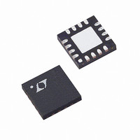
LTC6404HUD-1#TRPBF Linear Technology, LTC6404HUD-1#TRPBF Datasheet - Page 22

LTC6404HUD-1#TRPBF
Manufacturer Part Number
LTC6404HUD-1#TRPBF
Description
IC AMP/DRIVER DIFF 16-QFN
Manufacturer
Linear Technology
Type
ADC Driverr
Datasheet
1.LTC6404CUD-1PBF.pdf
(28 pages)
Specifications of LTC6404HUD-1#TRPBF
Applications
Data Acquisition
Mounting Type
Surface Mount
Package / Case
16-WQFN Exposed Pad
Current - Supply
27.8mA
Operating Temperature
-40°C ~ 125°C
Output Type
Differential, Rail-to-Rail
Number Of Circuits
1
Current - Output / Channel
85mA
Amplifier Type
Differential
Voltage - Supply, Single/dual (±)
2.7 V ~ 5.5 V, ±1.35 V ~ 2.75 V
-3db Bandwidth
600MHz
Slew Rate
450 V/µs
Gain Bandwidth Product
500MHz
Current - Input Bias
23µA
Voltage - Input Offset
500µV
Lead Free Status / RoHS Status
Lead free / RoHS Compliant
Available stocks
Company
Part Number
Manufacturer
Quantity
Price
APPLICATIONS INFORMATION
LTC6404
According to Figure 4, the input impedance looking into
the differential amp (R
case, thus:
R2 is chosen to balance R1 || R
Input Common Mode Voltage Range
The LTC6404’s input common mode voltage (V
defi ned as the average of the two input voltages, V
V
input common mode range depends on the circuit con-
fi guration (gain), V
fully differential input applications, where V
the common mode input voltage is approximately:
22
IN
R
R
–
V
V
. It extends from V
ICM
INM
CM
2
=
•
=
R
=
R R
⎛
⎝ ⎜
I
I
V
⎛
⎜
⎝
R
+
•
IN
1
F
R
R
– •
+
+ +
S
S
F
2
+
1
2
R
I
V
⎞
⎠ ⎟
⎛
⎝ ⎜
IN
OCM
R
R
–
I
INM
I
R
V
≈
+
–
CM
V
V
and V
F
INM
to 1.4V below V
V
INP
R
) refl ects the single ended source
OCM
F
+
–
–
+
⎞
⎠ ⎟
⎞
⎟
⎠
CM
V
V
•
VOCM
0.01μF
SHDN
0.1μF
S
⎛
⎝ ⎜
V
V
:
(Refer to Figure 5). For
R
+
–
I
R
+
I
R
F
1
2
3
4
Figure 5. Circuit for Common Mode Range
+
SHDN
V
V
V
⎞
⎠ ⎟
. The operating
+
–
OCM
+
R
R
16
V
V
INP
5
I
I
SHDN
+
–
NC
NC
= –V
IN
ICM
15
6
+
, and
INM
IN
IN
) is
+
–
V
+
–
R
R
OCM
F
F
,
14
7
With singled ended inputs, there is an input signal com-
ponent to the input common mode voltage. Applying only
V
approximately:
Output Common Mode Voltage Range
The output common mode voltage is defi ned as the aver-
age of the two outputs:
The V
mode feedback loop which internally forces V
The output common mode range extends from 1.1V above
V
for the LTC6404-4 output common mode voltage range).
The V
sets the default mid-supply open circuit potential.
OUT
OUT
INP
–
to 1V below V
V
V
V
–
+
V
V
ICM
CM
OUTCM
(setting V
OUTF
OUTF
13
OCM
OCM
8
•
–
+
OUTF
OUTF
=
⎛
⎝ ⎜
V
pin sits in the middle of a voltage divider which
+
V
LTC6404
R
pin sets this average by an internal common
=
–
+
IN
V
V
F
–
–
R
6404 F05
V
+
+ +
F
V
V
V
V
INM
OCM
–
+
+
–
+
2
R
12
11
10
9
+
I
V
(see the Electrical Characteristics table
⎞
⎠ ⎟
IN
to zero), the input common voltage is
V
V
=
+
OUT
OUT
–
V
0.1μF
0.1μF
V
–
+
≈
OUT
INP
2
V
OCM
+
•
+
⎛
⎝ ⎜
2
0.1μF
0.1μF
0.1μF
R
V
•
V
V
V
OUT
⎛
⎝ ⎜
F
+
–
–
R
R
+
F
I
R
–
R
+
I
I
R
⎞
⎠ ⎟
F
⎞
⎠ ⎟
OUT
+
+
= –V
OUT
6404f
–
.


