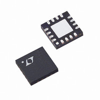
LTC6404HUD-1#TRPBF Linear Technology, LTC6404HUD-1#TRPBF Datasheet - Page 26

LTC6404HUD-1#TRPBF
Manufacturer Part Number
LTC6404HUD-1#TRPBF
Description
IC AMP/DRIVER DIFF 16-QFN
Manufacturer
Linear Technology
Type
ADC Driverr
Datasheet
1.LTC6404CUD-1PBF.pdf
(28 pages)
Specifications of LTC6404HUD-1#TRPBF
Applications
Data Acquisition
Mounting Type
Surface Mount
Package / Case
16-WQFN Exposed Pad
Current - Supply
27.8mA
Operating Temperature
-40°C ~ 125°C
Output Type
Differential, Rail-to-Rail
Number Of Circuits
1
Current - Output / Channel
85mA
Amplifier Type
Differential
Voltage - Supply, Single/dual (±)
2.7 V ~ 5.5 V, ±1.35 V ~ 2.75 V
-3db Bandwidth
600MHz
Slew Rate
450 V/µs
Gain Bandwidth Product
500MHz
Current - Input Bias
23µA
Voltage - Input Offset
500µV
Lead Free Status / RoHS Status
Lead free / RoHS Compliant
Available stocks
Company
Part Number
Manufacturer
Quantity
Price
APPLICATIONS INFORMATION
LTC6404
other external sources of noise from being converted to
differential noise due to divider mismatches in the feedback
networks. It is also recommended that the resistive feed-
back networks be comprised of 1% resistors (or better)
to enhance the output common mode rejection. This will
also prevent V
common mode amplifi er path (which cannot be fi ltered)
from being converted to differential noise, degrading the
differential noise performance.
Feedback factor mismatch has a weak effect on distortion.
Using 1% or better resistors should prevent mismatch
from impacting amplifi er linearity. However, in single
supply level shifting applications where there is a voltage
difference between the input common mode voltage and
the output common mode voltage, resistor mismatch can
make the apparent voltage offset of the amplifi er appear
worse than specifi ed.
In general, the apparent input referred offset induced by
feedback factor mismatch is given by the equation:
where
26
V
Δβ =
OSDIFF(APPARENT)
R
3.3V
0.1μF
0.1μF
I
2
R
+
I
2
R
OCM
F
2V
2
V
IN
P-P
1
2
3
4
–
referred common mode noise of the
SHDN
V
V
V
+
–
OCM
R
≈ (V
I
16
V
V
1
5
SHDN
+
–
R
+
100Ω
100Ω
NC
NC
I
INCM
1
R
F
1
15
Figure 11. Interfacing the LTC6404-1 to a High Speed 105Msps ADC
6
– V
IN
IN
100Ω
100Ω
+
–
V
+
–
OCM
OCM
) • Δβ
14
7
OUT
OUT
–
+
13
8
OUTF
OUTF
LTC6404-1
V
+
–
+
V
V
–
–
6404 F11
V
V
V
V
–
+
+
–
12
11
10
9
Interfacing the LTC6404 to A/D Converters
The LTC6404’s rail-to-rail output and fast settling time make
the LTC6404 ideal for interfacing to low voltage, single
supply, differential input ADCs. The sampling process of
ADCs create a sampling glitch caused by switching in the
sampling capacitor on the ADC front end which momentarily
“shorts” the output of the amplifi er as charge is transferred
between the amplifi er and the sampling cap. The amplifi er
must recover and settle from this load transient before
this acquisition period ends for a valid representation of
the input signal. In general, the LTC6404 will settle much
more quickly from these periodic load impulses than
from a 2V input step, but it is a good idea to either use
the fi ltered outputs to drive the ADC (Figure 11 shows an
example of this), or to place a discrete R-C fi lter network
between the differential unfi ltered outputs of the LTC6404
and the input of the ADC to help absorb the charge transfer
required during the ADC sampling process. The capaci-
tance of the fi lter network serves as a charge reservoir
to provide high frequency charging during the sampling
process, while the two resistors of the fi lter network are
used to dampen and attenuate any charge kickback from
the ADC. The selection of the R-C time constant is trial
and error for a given ADC, but the following guidelines
are recommended: Choosing too large of a resistor in the
decoupling network (leaving insuffi cient settling time)
0.1μF
0.1μF
3.3V
V
CM
2.2μF
AIN
AIN
+
–
LTC2207
GND
CONTROL
V
DD
D15
D0
•
•
1μF
1μF
3.3V
6404f


