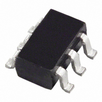
AD8027ARTZ-R2 Analog Devices Inc, AD8027ARTZ-R2 Datasheet - Page 3

AD8027ARTZ-R2
Manufacturer Part Number
AD8027ARTZ-R2
Description
IC OPAMP R-R LDIST LN LP SOT23-6
Manufacturer
Analog Devices Inc
Datasheet
1.AD8027ARZ.pdf
(24 pages)
Specifications of AD8027ARTZ-R2
Slew Rate
100 V/µs
Amplifier Type
Voltage Feedback
Number Of Circuits
1
Output Type
Rail-to-Rail
-3db Bandwidth
190MHz
Current - Input Bias
4µA
Voltage - Input Offset
200µV
Current - Supply
6.5mA
Current - Output / Channel
120mA
Voltage - Supply, Single/dual (±)
2.7 V ~ 12 V, ±1.35 V ~ 6 V
Operating Temperature
-40°C ~ 125°C
Mounting Type
Surface Mount
Package / Case
SOT-23-6
Op Amp Type
Low Distortion
No. Of Amplifiers
1
Bandwidth
190MHz
Supply Voltage Range
2.7V To 12V
Amplifier Case Style
SOT-23
No. Of Pins
6
Lead Free Status / RoHS Status
Lead free / RoHS Compliant
Gain Bandwidth Product
-
Lead Free Status / RoHS Status
Lead free / RoHS Compliant, Lead free / RoHS Compliant
Other names
AD8027ARTZ-R2TR
Available stocks
Company
Part Number
Manufacturer
Quantity
Price
Part Number:
AD8027ARTZ-R2
Manufacturer:
ADI/亚德诺
Quantity:
20 000
SPECIFICATIONS
V
Table 1.
Parameter
DYNAMIC PERFORMANCE
NOISE/DISTORTION PERFORMANCE
DC PERFORMANCE
INPUT CHARACTERISTICS
SELECT PIN
OUTPUT CHARACTERISTICS
POWER SUPPLY
1
No sign or a plus sign indicates current into the pin; a minus sign indicates current out of the pin.
S
–3 dB Bandwidth
Bandwidth for 0.1 dB Flatness
Slew Rate
Settling Time to 0.1%
Spurious-Free Dynamic Range (SFDR)
Input Voltage Noise
Input Current Noise
Differential Gain Error
Differential Phase Error
Crosstalk, Output to Output
Input Offset Voltage
Input Offset Voltage Drift
Input Bias Current
Input Offset Current
Open-Loop Gain
Input Impedance
Input Capacitance
Input Common-Mode Voltage Range
Common-Mode Rejection Ratio
Crossover Low, Selection Input Voltage
Crossover High, Selection Input Voltage
Disable Input Voltage
Disable Switching Speed
Enable Switching Speed
Output Overdrive Recovery Time
Output Voltage Swing
Short-Circuit Output
Off Isolation
Capacitive Load Drive
Operating Range
Quiescent Current/Amplifier
Quiescent Current (Disabled)
Power Supply Rejection Ratio
= ±5 V at T
(Rising/Falling Edge)
A
= 25°C, R
1
L
= 1 kΩ to midsupply, G = 1, unless otherwise noted.
Conditions
G = 1, V
G = 1, V
G = 2, V
G = +1, V
G = 2, V
f
f
f = 100 kHz
f = 100 kHz
NTSC, G = 2, R
NTSC, G = 2, R
G = 1, R
V
SELECT = three-state or open, PNP active
SELECT = high NPN active
T
V
T
V
T
V
V
Three-state < ±20 μA
50% of input to <10% of final V
V
Sinking and Sourcing
V
30% overshoot
SELECT = low
V
C
C
MIN
MIN
MIN
S
CM
CM
O
CM
I
IN
S
= 1 MHz, V
= 5 MHz, V
= +6 V to −6 V, G = −1
= ±5 V @ 1 MHz
± 1 V
= ±2.5 V
= 0.2 V p-p, f = 1 MHz, SELECT = low
= 0 V, NPN active
= 0 V, PNP active
= ±2.5 V
to T
to T
to T
O
O
O
O
L
MAX
MAX
MAX
= 100 Ω, V
O
= 0.2 V p-p
= 2 V p-p
= 0.2 V p-p
= 2 V step
= 2 V step/G = −1, V
O
O
L
= 2 V p-p, R
= 2 V p-p, R
L
= 150 Ω
= 150 Ω
Rev. C | Page 3 of 24
OUT
= 2 V p-p,
F
F
= 24.9 Ω
= 24.9 Ω
O
O
= 2 V step
Min
138
20
100
90
−V
2.7
90
S
+ 0.10
Typ
190
32
16
90/100
35
120
80
4.3
1.6
0.1
0.2
−93
200
240
1.50
4
4
−8
−8
±0.1
110
6
2
−5.2 to +5.2
110
−3.3 to +5
−3.9 to −3.3
−5 to −3.9
980
45
40/45
+V
−V
120
−49
20
6.5
370
110
S
S
− 0.06,
+ 0.06
AD8027/AD8028
Max
6
−11
±0.9
+V
12
8.5
800
900
500
S
− 0.10
Unit
MHz
MHz
MHz
V/μs
ns
dBc
dBc
nV/√Hz
pA/√Hz
%
Degrees
dB
μV
μV
μV/°C
μA
μA
μA
μA
μA
dB
MΩ
pF
V
dB
V
V
V
ns
ns
ns
V
mA
dB
pF
V
mA
μA
dB


