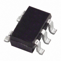
AD8009JRTZ-R2 Analog Devices Inc, AD8009JRTZ-R2 Datasheet - Page 13

AD8009JRTZ-R2
Manufacturer Part Number
AD8009JRTZ-R2
Description
IC OPAMP CF LDIST 175MA SOT23-5
Manufacturer
Analog Devices Inc
Datasheet
1.AD8009JRTZ-REEL7.pdf
(16 pages)
Specifications of AD8009JRTZ-R2
Slew Rate
5500 V/µs
Amplifier Type
Current Feedback
Number Of Circuits
1
-3db Bandwidth
845MHz
Current - Input Bias
50µA
Voltage - Input Offset
2000µV
Current - Supply
16mA
Current - Output / Channel
175mA
Voltage - Supply, Single/dual (±)
5 V ~ 12 V, ±2.5 V ~ 6 V
Operating Temperature
0°C ~ 70°C
Mounting Type
Surface Mount
Package / Case
SOT-23-5, SC-74A, SOT-25
Op Amp Type
Current Feedback
No. Of Amplifiers
1
Bandwidth
1GHz
Supply Voltage Range
± 5V To ± 6V
Amplifier Case Style
SOT-23
No. Of Pins
5
Lead Free Status / RoHS Status
Lead free / RoHS Compliant
Output Type
-
Gain Bandwidth Product
-
Lead Free Status / RoHS Status
Lead free / RoHS Compliant, Lead free / RoHS Compliant
Other names
AD8009JRTZ-R2TR
Driving a Capacitive Load
A capacitive load, like that presented by some A/D converters,
can sometimes be a challenge for an op amp to drive depending
on the architecture of the op amp. Most of the problem is caused
by the pole created by the output impedance of the op amp and
the capacitor that is driven. This creates extra phase shift that
can eventually cause the op amp to become unstable.
One way to prevent instability and improve settling time when
driving a capacitor is to insert a resistor in series between the
op amp output and the capacitor. The feedback resistor is still
connected directly to the output of the op amp, while the series
resistor provides some isolation of the capacitive load from the
op amp output.
REV. F
G = +10: R
G = +2: R
Figure 5. Capacitive Load Drive Circuit
F
F
= 301
= 200 , R
R
T
49.9
= R
G
G
R
= 22.1
G
3
2
AD8009
R
+5V
F
–5V
7
4
0.001 F
6
0.001 F
2V
STEP
0.1 F
R
0.1 F
S
C
L
+
10 F
+
10 F
50pF
–13–
Figure 5 shows such a circuit with an AD8009 driving a 50 pF
load. With R
gain of +2 and +10, it was found experimentally that setting R
to 42.2 Ω will minimize the 0.1% settling time with a 2 V step at
the output. The 0.1% settling time was measured to be 40 ns with
this circuit.
For smaller capacitive loads, a smaller R
settling time, while a larger R
loads. Of course, a larger capacitance will always require more
time for settling to a given accuracy than a smaller one, and this
will be lengthened by the increase in R
given RC combination will require about seven time constants
by itself to settle to 0.1%, so a limit will be reached where too
large a capacitance cannot be driven by a given op amp and still
meet the system’s required settling time specification.
S
= 0, the AD8009 circuit will be unstable. For a
S
will be required for larger capacitive
S
required. At best, a
S
will yield optimal
AD8009
S


