AD215BY Analog Devices Inc, AD215BY Datasheet
AD215BY
Specifications of AD215BY
Available stocks


Related parts for AD215BY


AD215BY Summary of contents
Page 1
... The AD215 provides designers with complete isolation of the desired signal without loss of signal integrity or quality. Excellent Common-Mode Performance: The AD215BY (AD215AY) provides 1,500 V rms (750 V rms) common-mode voltage protection from its input to output. Both grades feature a low common-mode capacitance of 4.5 pF inclusive of the dc/dc power isolation ...
Page 2
... AD215BY Grade AD215AY Grade INPUT VOLTAGE RATINGS Input Voltage Rating Maximum Safe Differential Range CMRR of Input Op Amp 4 Isolation Voltage Rating AD215BY Grade AD215AY Grade IMRR (Isolation Mode Rejection Ratio) Leakage Current, Input to Output INPUT IMPEDANCE Differential Common Mode INPUT OFFSET VOLTAGE Initial vs ...
Page 3
Parameter DYNAMIC RESPONSE (2 k Load) Cont. Settling Time Overshoot Harmonic Distortion Components Overload Recovery Time Output Overload Recovery Time RATED OUTPUT Voltage Current Max Capacitive Load Output Resistance 7 Output Ripple and Noise 8 ISOLATED POWER OUTPUT Voltage vs. ...
Page 4
... Output High 42 + Power IN 43 PWR RTN Power Supply Common 44 –15 V – Power IN ORDERING GUIDE Model Temperature Range V AD215AY – +85 C 750 AD215BY – +85 C 1500 *Typical @ + V/V. SIGNAL LOW-PASS FILTER MODULATOR DEMODULATOR 150kHz T1 POWER 430kHz ISOLATED POWER DC OSCILLATOR SUPPLY T2 Figure 1. Functional Block Diagram ...
Page 5
TEMPERATURE – C Figure 2. Gain Error vs. Temperature 1mV 100 – –10 –8 –6 –4 – OUTPUT VOLTAGE ...
Page 6
AD215–Performance Characteristics 100 90 100mV 5µs OVERSHOOT Figure 7a. Overshoot to a Full-Scale Step Input ( V/V) 100 90 5V 100mV 10 0% 5µs UNDERSHOOT Figure 7b. Undershoot to a Full-Scale Input ( ...
Page 7
POWERING THE AD215 The AD215 is powered by a bipolar power supply connected as shown in Figure 11. External bypass capacitors should be provided in bused applications. Note that a small signal-related current (50 mA/V ) will ...
Page 8
AD215 Compensating the Uncommitted Input Op Amp The open-loop gain and phase versus frequency for the uncom- mitted input op amp are given in Figure 14. These curves can be used to determine appropriate values for the feedback resis- tor ...
Page 9
Input Gain Adjustments for the Inverting Mode Figure 17 shows a suggested inverting gain adjustment circuit. In this circuit, gain adjustment is made using a potentiometer ( the feedback loop. The adjustments are effective for all P gains ...
Page 10
AD215 When gain setting resistors are used, 0.325" channel centers can still be achieved as shown in Figure 20b COM ISO – ...
Page 11
ISO 220 1/2 AD648 350 + +V 350 ISO – 10k 6.8k 500 9.76k 220 1/2 AD589 AD648 –V –V ISO Figure 23. Strain Gage Signal Conditioning Application REV. 0 ISO Q1 –V ISO 2N3904 1M +1.2V FB ...
Page 12
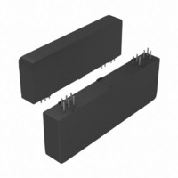
AD215 0.020 (0.5) 0.015 (0.4) 0.05 (1.3) 0.325 (8.3) MAX OUTLINE DIMENSIONS Dimensions shown in inches and (mm). AD215 SIP PACKAGE 2.480 (63.0) MAX 0.12 (3.0) TYP 0.094 (2.4) 0.16 (4.1) 0.16 (4.1) 2.15 (54.6) 0.2 (5.1) 0.250 (6.4) 0.1 ...