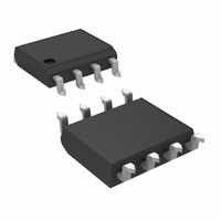
LMP7718MAE/NOPB National Semiconductor, LMP7718MAE/NOPB Datasheet - Page 14

LMP7718MAE/NOPB
Manufacturer Part Number
LMP7718MAE/NOPB
Description
IC OP AMP PREC DUAL 88MHZ 8-SOIC
Manufacturer
National Semiconductor
Series
LMP®, PowerWise®r
Datasheet
1.LMP7717MFNOPB.pdf
(24 pages)
Specifications of LMP7718MAE/NOPB
Amplifier Type
General Purpose
Number Of Circuits
2
Output Type
Rail-to-Rail
Slew Rate
35 V/µs
Gain Bandwidth Product
88MHz
Current - Input Bias
0.1pA
Voltage - Input Offset
10µV
Current - Supply
1.3mA
Current - Output / Channel
60mA
Voltage - Supply, Single/dual (±)
1.8 V ~ 5.5 V, ±0.9 V ~ 2.75 V
Operating Temperature
-40°C ~ 125°C
Mounting Type
Surface Mount
Package / Case
8-SOIC (3.9mm Width)
Lead Free Status / RoHS Status
Lead free / RoHS Compliant
-3db Bandwidth
-
Other names
LMP7718MAE
www.national.com
What is a Decompensated Op Amp?
The differences between the unity gain stable op amp and the
decompensated op amp are shown in
assumes an ideal two pole system. The dominant pole of the
decompensated op amp is at a higher frequency, f
pared to the unity gain stable op amp which is at f
in
bility of the op amp while maintaining the same power dissi-
pation of the unity gain stable op amp. The LMP7717/
LMP7718 have a dominant pole at 1.6 kHz. The unity gain
stable LMP7715/LMP7716 have their dominant pole at
300 Hz.
FIGURE 3. Open Loop Gain for Unity Gain Stable Op Amp
Having a higher frequency for the dominate pole will result in:
1.
2.
3.
The second open loop pole (f
occurs at 45 MHz. The unity gain (f
pole at 51 MHz. An ideal two pole system would give a phase
margin of 45° at the location of the second pole. The
LMP7717/LMP7718 have parasitic poles close to the second
pole, giving a phase margin closer to 0°. Therefore it is nec-
essary to operate the LMP7717/LMP7718 at a closed loop
gain of 10 or higher, or to add external compensation in order
to assure stability.
For the LMP7715, the gain bandwidth product occurs at 17
MHz. The curve is constant from f
the second pole.
For the LMP7717/LMP7718 the GBW = 88 MHz and is con-
stant between f
A
frequency of 88 MHz. For decompensated op amps the unity
gain frequency and the GBW are no longer equal. G
minimum gain for stability and for the LMP7717/LMP7718 this
is a gain of 18 to 20 dB.
Input Lead-Lag Compensation
The recommended technique which allows the user to com-
pensate the LMP7717/LMP7718 for stable operation at any
gain is lead-lag compensation. The compensation compo-
nents added to the circuit allow the user to shape the feedback
function to make sure there is sufficient phase margin when
VOL
Figure
The DC open loop gain (A
frequency.
A wider closed loop bandwidth.
Better slew rate due to reduced compensation
capacitance within the op amp.
=1. Therefore f
3. This is done in order to increase the speed capa-
and Decompensated Op Amp
1
and f
u
’ occurs at 51 MHz, well before the GBW
2
. The second pole at f
2
VOL
) for the LMP7717/LMP7718
) extending to a higher
d
u
’) occurs after the second
to f
Figure
u
which occurs before
3. This Bode plot
2
occurs before
d
1
as shown
, as com-
min
30010824
is the
14
the loop gain is as low as 0 dB and still maintain the advan-
tages over the unity gain op amp.
lag configuration. Only R
compensation.
To cover how to calculate the compensation network values
it is necessary to introduce the term called the feedback factor
or F. The feedback factor F is the feedback voltage V
across the op amp input terminals relative to the op amp out-
put voltage V
From feedback theory the classic form of the feedback equa-
tion for op amps is:
A is the open loop gain of the amplifier and AF is the loop gain.
Both are highly important in analyzing op amps. Normally AF
>>1 and so the above equation reduces to:
Deriving the equations for the lead-lag compensation is be-
yond the scope of this datasheet. The derivation is based on
the feedback equations that have just been covered. The in-
verse of feedback factor for the circuit in
where 1/F's pole is located at
1/F's zero is located at
FIGURE 4. LMP7717 with Lead-Lag Compensation for
OUT
.
Inverting Configuration
C
and C are added for the necessary
Figure 4
Figure 4
shows the lead-
30010825
is:
A
-V
(1)
(2)
(3)
B


