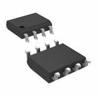
LMP7718MAE/NOPB National Semiconductor, LMP7718MAE/NOPB Datasheet - Page 18

LMP7718MAE/NOPB
Manufacturer Part Number
LMP7718MAE/NOPB
Description
IC OP AMP PREC DUAL 88MHZ 8-SOIC
Manufacturer
National Semiconductor
Series
LMP®, PowerWise®r
Datasheet
1.LMP7717MFNOPB.pdf
(24 pages)
Specifications of LMP7718MAE/NOPB
Amplifier Type
General Purpose
Number Of Circuits
2
Output Type
Rail-to-Rail
Slew Rate
35 V/µs
Gain Bandwidth Product
88MHz
Current - Input Bias
0.1pA
Voltage - Input Offset
10µV
Current - Supply
1.3mA
Current - Output / Channel
60mA
Voltage - Supply, Single/dual (±)
1.8 V ~ 5.5 V, ±0.9 V ~ 2.75 V
Operating Temperature
-40°C ~ 125°C
Mounting Type
Surface Mount
Package / Case
8-SOIC (3.9mm Width)
Lead Free Status / RoHS Status
Lead free / RoHS Compliant
-3db Bandwidth
-
Other names
LMP7718MAE
www.national.com
than the fully compensated parts.
1, or the buffer configuration, for these parts.
Figure 13
perimentation in the lab. R
necessary to introduce another pole at the input stage for
good performance at gain = +1. Equation 5 is shown below
with R
Using 2 kΩ for R
290Ω. The closest standard value for R
fine tuning in the lab R
as the optimum values. R
at the non-inverting pin inserts another pole into the compen-
sation for the LMP7717. Adding this pole and slightly reducing
the compensation for 1/F (using a slightly higher resistor value
for R
14
15
uration with no compensation and R
FIGURE 13. LMP7717 with Lead-Lag Compensation for
shows the response of the LMP7715 in the buffer config-
is the response of the circuit shown in
FIGURE 14. R
C
) gives the optimum response for a gain of +1.
IN
=
is the result of using Equation 5 and additional ex-
∞
.
Non-Inverting Configuration
F
and solving for R
C
= 330Ω and C = 10 nF, Gain = +1
C
= 330Ω and R
P
together with the input capacitance
P
is not part of Equation 5, but it is
Figure 13
C
P
P
= R
gives R
= 1.5 kΩ were chosen
C
is 300Ω. After some
F
Figure
= 0.
shows the gain =
C
30010884
= 2000/6.9 =
13.
30010888
Figure
Figure
18
With no increase in power consumption the decompensated
op amp offers faster speed than the compensated equivalent
part . These examples used R
enough to be easily driven by the LMP7717/LMP7718, yet
small enough to minimize the effects from the parasitic ca-
pacitance of both the PCB and the op amp.
Note: When using the LMP7717/LMP7718, proper high fre-
quency PCB layout must be followed. The GBW of these parts
is 88 MHz, making the PCB layout significantly more critical
than when using the compensated counterparts which have
a GBW of 17 MHz.
TRANSIMPEDANCE AMPLIFIER
An excellent application for either the LMP7717 or the
LMP7718 is as a transimpedance amplifier. With a GBW
product of 88 MHz these parts are ideal for high speed data
transmission by light. The circuit shown on the front page of
the
LMP7717/LMP7718 as transimpedance amplifiers. The only
change is that V
tion of the diode is reversed from the circuit shown on the front
page.
Very high speed components were used in testing to check
the limits of the LMP7717/LMP7718 in a transimpedance
configuration. The photodiode part number is PIN-HR040
from OSI Optoelectronics. The diode capacitance for this part
is only about 7 pF for the 2.5V bias used (V
ground). The rise time for this diode is 1 nsec. A laser diode
was used for the light source. Laser diodes have on and off
times under 5 nsec. The speed of the selected optical com-
ponents allowed an accurate evaluation of the LMP7717 as
a transimpedance amplifier. Nationals evaluation board for
decompensated op amps, PN 551013271-001 A, was used
and only minor modifications were necessary and no traces
had to be cut.
datasheet
FIGURE 15. LMP7715 Response Gain = +1
B
is tied to the V
is
the
circuit
F
CC
= 2 kΩ. This value is high
of the part, thus the direc-
used
to
CC
test
30010889
to virtual
the


