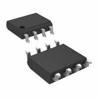
LMC662AIM/NOPB National Semiconductor, LMC662AIM/NOPB Datasheet

LMC662AIM/NOPB
Specifications of LMC662AIM/NOPB
Related parts for LMC662AIM/NOPB
LMC662AIM/NOPB Summary of contents
Page 1
... DIP/SO Ordering Information Package 8-Pin Small Outline 8-Pin Molded DIP © 2003 National Semiconductor Corporation Features n Rail-to-rail output swing n Specified for 2 kΩ and 600Ω loads n High voltage gain: n Low input offset voltage Low offset voltage drift: 1.3 µV/˚C ...
Page 2
... Absolute Maximum Ratings If Military/Aerospace specified devices are required, please contact the National Semiconductor Sales Office/ Distributors for availability and specifications. Differential Input Voltage + − Supply Voltage (V − Output Short Circuit to V − Output Short Circuit to V Lead Temperature (Soldering, 10 sec.) Storage Temp. Range ...
Page 3
DC Electrical Characteristics Unless otherwise specified, all limits guaranteed for T − 0V 1.5V 2.5V and Parameter + Output Swing kΩ ...
Page 4
AC Electrical Characteristics Unless otherwise specified, all limits guaranteed for T − 0V 1.5V 2.5V and Parameter Total Harmonic Distortion kHz Note 1: Applies to ...
Page 5
Typical Performance Characteristics Supply Current vs. Supply Voltage Input Bias Current Output Characteristics Current Sourcing ± 7.5V 25˚C unless otherwise specified S A 00976324 Output Characteristics Current Sinking 00976326 Input Voltage Noise vs. Frequency 00976328 5 ...
Page 6
Typical Performance Characteristics CMRR vs. Frequency Frequency Response vs. Capacitive Load Stability vs. Capacitive Load Note: Avoid resistive loads of less than 500Ω, as they may cause instability. www.national.com ± 7.5V 25˚C unless otherwise specified (Continued) ...
Page 7
Application Hints AMPLIFIER TOPOLOGY The topology chosen for the LMC662, shown in Figure 1, is unconventional (compared to general-purpose op amps) in that the traditional unity-gain buffer output stage is not used; instead, the output is taken directly from the ...
Page 8
Application Hints (Continued) Note that these capacitor values are usually significantly smaller than those given by the older, more conservative formula: C consists of the amplifier’s input capacitance plus any stray capacitance S from the circuit board and socket. C ...
Page 9
Application Hints (Continued) dard op-amp configurations. If both inputs are active and at high impedance, the guard can be tied to ground and still provide some protection; see Figure 9. FIGURE 5. Example, using the LMC660, of Guard Ring in ...
Page 10
Application Hints (Continued) BIAS CURRENT TESTING The test method of Figure 11 is appropriate for bench-testing bias current with reasonable accuracy. To understand its operation, first close switch S2 momentarily. When S2 is opened, then FIGURE 11. Simple Input Bias ...
Page 11
Typical Single-Supply Applications + ( Additional single-supply applications ideas can be found in the LM358 datasheet. The LMC662 is pin-for-pin compatible with the LM358 and offers greater bandwidth and input resistance over the LM358. These ...
Page 12
Typical Single-Supply Applications ( 5 (Continued Bandpass Filter 2.1 Gain = −8 High-Pass Filter 0.895 Gain = ...
Page 13
Physical Dimensions inches (millimeters) unless otherwise noted Order Number LMC662AIM, LMC662CM, LMC662AIMX or LMC662CMX Small Outline Dual-In-Line Pkg. (M) NS Package Number M08A Molded Dual-In-Line Pkg. (N) Order Number LMC662AIN, LMC662CN NS Package Number N08E 13 www.national.com ...
Page 14
... NATIONAL’S PRODUCTS ARE NOT AUTHORIZED FOR USE AS CRITICAL COMPONENTS IN LIFE SUPPORT DEVICES OR SYSTEMS WITHOUT THE EXPRESS WRITTEN APPROVAL OF THE PRESIDENT AND GENERAL COUNSEL OF NATIONAL SEMICONDUCTOR CORPORATION. As used herein: 1. Life support devices or systems are devices or systems which, (a) are intended for surgical implant ...


