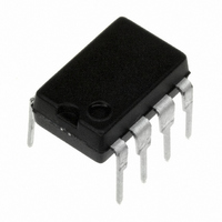
LM6181IN/NOPB National Semiconductor, LM6181IN/NOPB Datasheet - Page 23

LM6181IN/NOPB
Manufacturer Part Number
LM6181IN/NOPB
Description
IC AMP CUR FEEDBACK 100MHZ 8-DIP
Manufacturer
National Semiconductor
Series
VIP™ IIr
Datasheet
1.LM6181IM-8NOPB.pdf
(28 pages)
Specifications of LM6181IN/NOPB
Amplifier Type
Current Feedback
Number Of Circuits
1
Slew Rate
2000 V/µs
-3db Bandwidth
100MHz
Current - Input Bias
5µA
Voltage - Input Offset
3500µV
Current - Supply
7.5mA
Current - Output / Channel
130mA
Voltage - Supply, Single/dual (±)
7 V ~ 32 V, ±3.5 V ~ 16 V
Operating Temperature
-40°C ~ 85°C
Mounting Type
Through Hole
Package / Case
8-DIP (0.300", 7.62mm)
Number Of Channels
1
Common Mode Rejection Ratio (min)
50 dB
Input Offset Voltage
3 mV at +/- 5 V
Operating Supply Voltage
9 V, 12 V, 15 V, 18 V, 24 V, 28 V
Supply Current
8.5 mA at +/- 5 V
Maximum Operating Temperature
+ 85 C
Maximum Dual Supply Voltage
+/- 16 V
Minimum Operating Temperature
- 40 C
Lead Free Status / RoHS Status
Lead free / RoHS Compliant
Output Type
-
Gain Bandwidth Product
-
Lead Free Status / Rohs Status
Details
Other names
*LM6181IN
*LM6181IN/NOPB
LM6181IN
*LM6181IN/NOPB
LM6181IN
Typical Applications
CAPACITIVE FEEDBACK
For voltage feedback amplifiers it is quite common to place a
small lead compensation capacitor in parallel with feedback
resistance, R
plifier’s peaking in the frequency domain which equivalently
tames the transient response. To limit the bandwidth of
current feedback amplifiers, do not use a capacitor across
R
loop reduces the amplifier’s stability. Instead, reduced peak-
ing in the frequency response, and bandwidth limiting can be
accomplished by adding an RC circuit, as illustrated in Fig-
ure 7b.
f
. The dynamic impedance of capacitors in the feedback
and R
and Improve Pulse Response Characteristics.
Provides Higher Fidelity Pulse Response. R
S
FIGURE 6. Resistive Isolation of C
Could Be Increased to Maintain A
f
. This compensation serves to reduce the am-
6a
6b
(Continued)
L
V
01132820
= −1
01132821
f
23
Typical Performance
Characteristics
OVERDRIVE RECOVERY
When the output or input voltage range of a high speed
amplifier is exceeded, the amplifier must recover from an
overdrive condition. The typical recovery times for open-
loop, closed-loop, and input common-mode voltage range
overdrive conditions are illustrated in Figures 9, 11, 11, 12
respectively.
The open-loop circuit of Figure 8 generates an overdrive
response by allowing the
input range of the amplifier. Typical positive and negative
overdrive recovery times shown in Figure 9 are 5 ns and
25 ns, respectively.
Peaking in the Resulting Pulse Response
Bandwidth to 50 MHz, Eliminating
FIGURE 7. RC Limits Amplifier
±
0.5V input to exceed the linear
7a
7b
www.national.com
01132822
01132823


