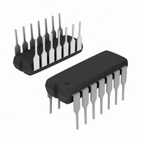
HA1-2540-5 Intersil, HA1-2540-5 Datasheet - Page 2

HA1-2540-5
Manufacturer Part Number
HA1-2540-5
Description
IC OP AMP 400MHZ MONO 14-CDIP
Manufacturer
Intersil
Datasheet
1.HA1-2540-5.pdf
(8 pages)
Specifications of HA1-2540-5
Amplifier Type
General Purpose
Number Of Circuits
1
Slew Rate
400 V/µs
Gain Bandwidth Product
400MHz
Current - Input Bias
5µA
Voltage - Input Offset
8000µV
Current - Supply
20mA
Current - Output / Channel
20mA
Voltage - Supply, Single/dual (±)
±5 V ~ 15 V
Operating Temperature
0°C ~ 75°C
Mounting Type
Through Hole
Package / Case
14-CDIP (0.300", 7.62mm)
Lead Free Status / RoHS Status
Contains lead / RoHS non-compliant
Output Type
-
-3db Bandwidth
-
Available stocks
Company
Part Number
Manufacturer
Quantity
Price
Part Number:
HA1-2540-5
Manufacturer:
HAR
Quantity:
20 000
Absolute Maximum Ratings
Voltage Between V+ and V- Terminals . . . . . . . . . . . . . . . . . . . 35V
Differential Input Voltage . . . . . . . . . . . . . . . . . . . . . . . . . . . . . . . 6V
Output Current . . . . . . . . . . . . . . 33mA
Operating Conditions
Temperature Range
CAUTION: Stresses above those listed in “Absolute Maximum Ratings” may cause permanent damage to the device. This is a stress only rating and operation of the
device at these or any other conditions above those indicated in the operational sections of this specification is not implied.
NOTES:
Electrical Specifications
INPUT CHARACTERISTICS
Offset Voltage
Average Offset Voltage Drift
Bias Current
Offset Current
Input Resistance
Input Capacitance
Common Mode Range
Input Noise Current (f = 1kHz, R
Input Noise Voltage (f = 1kHz, R
TRANSFER CHARACTERISTICS
Large Signal Voltage Gain (Note 3)
Common-Mode Rejection Ratio (Note 4)
Minimum Stable Gain
Gain Bandwidth Product (Notes 5, 6)
OUTPUT CHARACTERISTICS
Output Voltage Swing (Notes 3, 10)
Output Current (Note 3)
Output Resistance
Full Power Bandwidth (Notes 3, 7)
TRANSIENT RESPONSE (Note 8)
Rise Time
Overshoot
Slew Rate
Settling Time: 10V Step to 0.1%
1. Maximum power dissipation with load conditions must be designed to maintain the maximum junction temperature below 175
2. θ
HA-2540-5 . . . . . . . . . . . . . . . . . . . . . . . . . . . . . . . . 0
package, and below 150
resistances, proper load conditions can be determined. Heat sinking is recommended above 75
JA
is measured with the component mounted on an evaluation PC board in free air.
o
C for the plastic package. By using Application Note AN556 on Safe Operating Area Equations, along with the thermal
SOURCE
SOURCE
2
V
SUPPLY
RMS
PARAMETER
= 0Ω)
= 0Ω)
Continuous, 50mA
= ±15V, R
L
o
= 1kΩ, C
C to 75
PEAK
o
HA-2540
C
L
< 10pF, Unless Otherwise Specified
Thermal Information
Thermal Resistance (Typical, Note 2)
Maximum Internal Power Dissipation (Note 1)
Maximum Junction Temperature (Ceramic Package) . . . . . . 175
Maximum Storage Temperature Range . . . . . . . . . -65
Maximum Lead Temperature (Soldering 10s) . . . . . . . . . . . . 300
CERDIP Package. . . . . . . . . . . . . . . . .
TEMP (
Full
Full
Full
Full
Full
Full
Full
Full
25
25
25
25
25
25
25
25
25
25
25
25
25
25
25
25
25
o
o
C.
C)
MIN
±10
±10
±10
320
5.5
10
60
10
5
-
-
-
-
-
-
-
-
-
-
-
-
-
-
-
-
TYP
400
±20
400
140
13
20
10
15
72
30
14
6
8
5
1
1
6
6
5
-
-
-
-
-
-
θ
JA
(
75
o
C/W) θ
o
MAX
C for the ceramic
15
20
20
25
6
8
-
-
-
-
-
-
-
-
-
-
-
-
-
-
-
-
-
-
-
o
C to 150
JC
pA/√Hz
nV/√Hz
UNITS
µV/
kV/V
(
kV/V
MHz
MHz
V/µs
20
V/V
mV
mV
mA
o
µA
µA
µA
µA
kΩ
pF
dB
ns
ns
%
V
V
Ω
C/W)
o
C
o
o
o
C
C
C


