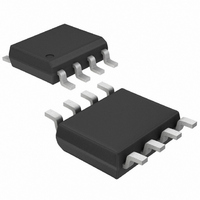
MAX4162ESA Maxim Integrated Products, MAX4162ESA Datasheet - Page 2

MAX4162ESA
Manufacturer Part Number
MAX4162ESA
Description
IC OPAMP MICROPWR SNGL R-R 8SOIC
Manufacturer
Maxim Integrated Products
Datasheet
1.MAX4162EUKT.pdf
(13 pages)
Specifications of MAX4162ESA
Amplifier Type
General Purpose
Number Of Circuits
1
Output Type
Rail-to-Rail
Slew Rate
0.115 V/µs
Gain Bandwidth Product
200kHz
Current - Input Bias
1pA
Voltage - Input Offset
500µV
Current - Supply
25µA
Current - Output / Channel
15mA
Voltage - Supply, Single/dual (±)
2.7 V ~ 10 V, ±1.35 V ~ 5 V
Operating Temperature
-40°C ~ 85°C
Mounting Type
Surface Mount
Package / Case
8-SOIC (3.9mm Width)
Number Of Channels
1
Voltage Gain Db
120 dB
Common Mode Rejection Ratio (min)
70 dB
Input Offset Voltage
3 mV
Operating Supply Voltage
3 V, 5, V, 9 V
Supply Current
0.025 mA
Maximum Power Dissipation
588 mW
Maximum Operating Temperature
+ 85 C
Mounting Style
SMD/SMT
Maximum Dual Supply Voltage
+/- 5 V
Minimum Operating Temperature
- 40 C
Lead Free Status / RoHS Status
Contains lead / RoHS non-compliant
-3db Bandwidth
-
Available stocks
Company
Part Number
Manufacturer
Quantity
Price
Company:
Part Number:
MAX4162ESA
Manufacturer:
MAXIM
Quantity:
27
Part Number:
MAX4162ESA
Manufacturer:
MAXIM/美信
Quantity:
20 000
Company:
Part Number:
MAX4162ESA+T
Manufacturer:
TOSHIBA
Quantity:
6 217
ABSOLUTE MAXIMUM RATINGS
Supply Voltage (V
IN+, IN-, OUT Voltage ......................(V
Short-Circuit Duration (to either rail)...........................Continuous
Continuous Power Dissipation (T
UCSP, Micropower, Single-Supply, 10V,
Rail-to-Rail I/O Op Amps
ELECTRICAL CHARACTERISTICS: 3V Operation
(V
ues are at T
Stresses beyond those listed under “Absolute Maximum Ratings” may cause permanent damage to the device. These are stress ratings only, and functional
operation of the device at these or any other conditions beyond those indicated in the operational sections of the specifications is not implied. Exposure to
absolute maximum rating conditions for extended periods may affect device reliability.
2
5-Pin SOT23 (derate 3.9mW/°C above +70°C)..............312mW
8-Pin SO (derate 7.4mW/°C above +70°C)....................588mW
8-Pin UCSP (derate 4.7mW/°C above +70°C) ...............379mW
Operating Voltage Range
Supply Current (Per Amplifier)
Input Bias Current (Note 2)
Input Offset Voltage
Input Offset Voltage Tempco
Differential Input Resistance
Input Common-Mode Voltage
Range
Common-Mode Rejection Ratio
Large-Signal Voltage Gain
Output Voltage Swing
Output Short-Circuit Current
Closed-Loop Output Resistance
Power-Supply Rejection Ratio
Gain-Bandwidth Product
Phase Margin
Gain Margin
Total Harmonic Distortion
Slew Rate
Settling Time to 0.1%
Turn-On Time
DD
_______________________________________________________________________________________
= 3V, V
PARAMETER
A
SS
= +25°C.) (Note 1)
= 0V, V
DD
to V
CM
SS
= V
) ..................................................11V
DD
A
/2, V
= +70°C)
SYMBOL
TCV
CMRR
GBWP
PSRR
R
V
THD
V
V
V
GM
t
OUT
I
R
I
φM
SR
A
OUT
DD
OUT
ON
DD
I
SC
CM
DD
OS
B
IN
V
OS
+ 0.3V) to (V
= V
DD
Inferred from PSRR test
MAX4162
MAX4163
MAX4164
Inferred from CMRR test
V
R
R
R
To either supply rail
A
V
f = 1kHz, V
V
V
CM
DD
OUT
DD
L
L
L
V
/2, R
= 10kΩ
= 10kΩ
= 100kΩ
= 1V/V
= 2.5V to 10V
= 0 to 3V step, V
= (V
= 1V to 2V step
L
SS
connected to V
SS
- 0.3V)
OUT
- 0.25V) to (V
T
T
T
T
T
T
V
V
V
V
= 2V
A
A
A
A
A
A
DD
OL
DD
OL
CONDITIONS
= +25°C
= -40°C to +85°C
= +25°C
= -40°C to +85°C
= +25°C
= -40°C to +85°C
- V
- V
- V
- V
P-P
IN
SS
SS
OH
OH
, R
Operating Temperature Range ...........................-40°C to +85°C
Storage Temperature Range .............................-65°C to +150°C
Junction Temperature ......................................................+150°C
Lead Temperature (soldering, 10s) .................................+300°C
Soldering Temperature (reflow, UCSP)............................+260°C
DD
= V
8-Pin µMAX (derate 4.8mW/°C above +70°C) ...............387mW
14-Pin SO (derate 12.3mW/°C above +70°C)................987mW
DD
L
/2, T
= 100kΩ, A
DD
+ 0.25V)
/2, A
A
= -40°C to +85°C, unless otherwise noted. Typical val-
V
= 1V/V
V
= 1V/V
V
0.25
MIN
2.5
SS
70
85
80
-
TYP
±0.5
±0.5
±0.5
0.02
>10
100
120
110
200
115
1.0
0.1
25
30
30
15
60
12
50
20
2
3
3
V
MAX
10.0
0.25
100
180
180
DD
40
±3
±4
±4
±5
±5
±6
25
25
+
degrees
UNITS
µV/°C
V/ms
kHz
mA
mV
mV
µA
pA
TΩ
dB
dB
dB
dB
µs
µs
%
Ω
V
V


