MAX4206ETE+T Maxim Integrated Products, MAX4206ETE+T Datasheet - Page 15

MAX4206ETE+T
Manufacturer Part Number
MAX4206ETE+T
Description
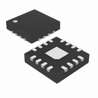
IC AMP TRANS LOG 16-TQFN
Manufacturer
Maxim Integrated Products
Datasheet
1.MAX4206ETET.pdf
(17 pages)
Specifications of MAX4206ETE+T
Amplifier Type
Logarithmic
Number Of Circuits
1
Slew Rate
12 V/µs
Gain Bandwidth Product
5MHz
Voltage - Input Offset
1000µV
Current - Supply
5mA
Current - Output / Channel
58mA
Voltage - Supply, Single/dual (±)
2.7 V ~ 11 V, ±2.7 V ~ 5.5 V
Operating Temperature
-40°C ~ 85°C
Mounting Type
Surface Mount
Package / Case
16-TQFN Exposed Pad
Number Of Channels
1
Input Offset Voltage
5 mV
Operating Supply Voltage
3 V, 5 V, 9 V
Supply Current
5 mA
Operating Temperature Range
+ 85 C
Mounting Style
SMD/SMT
Power Dissipation
1349 mW
Lead Free Status / RoHS Status
Lead free / RoHS Compliant
Output Type
-
-3db Bandwidth
-
Current - Input Bias
-
Lead Free Status / Rohs Status
Details
Figure 8 shows the MAX4206 in a single-supply, optical-
power measurement circuit, common in fiberoptic
applications. The MAX4007 current monitor converts
the sensed APD current to an output current that drives
the MAX4206 LOGIIN input (APD current is scaled by
0.1). The MAX4007 also buffers the high-voltage APD
voltages from the lower MAX4206 voltages. The
MAX4206’s internal current reference sources 10nA
(R
sets the logarithmic intercept to 10nA, corresponding to
an APD current of 100nA. The unity-gain configuration
of the output buffer maintains the 0.25V/decade gain
present at the LOGV1 output.
The MAX4206 drives capacitive loads of up to 50pF.
Reactive loads decrease phase margin and can pro-
duce excessive ringing and oscillation. Use an isolation
resistor in series with LOGV1 or LOGV2 to reduce the
effect of large capacitive loads. Recall that the combi-
nation of the capacitive load and the small isolation
resistor limits AC performance.
The LOGV1 and LOGV2 amplifiers are capable of
sourcing or sinking in excess of 30mA. Ensure that the
continuous power dissipation rating for the MAX4206 is
not exceeded.
The 16-lead thin QFN package has an exposed paddle
that provides a heat-removal path, as well as excellent
electrical grounding to the PC board. The MAX4206’s
exposed pad is internally connected to V
either be connected to the PC board V
unconnected. Ensure that only V
under the exposed paddle.
Bypass V
capacitors. Place the capacitors as close to the device
as possible. Bypass REFVOUT and/or CMVOUT to
GND with a 0.1µF ceramic capacitor for increased
Amplifier with Over 5 Decades of Dynamic Range
SET
= 5MΩ) to the REFIIN input. This configuration
CC
and V
Photodiode Current Monitoring
______________________________________________________________________________________
EE
Precision Transimpedance Logarithmic
to GND with ceramic 0.1µF
Layout and Bypassing
Power Dissipation
Capacitive Loads
EE
TQFN Package
traces are routed
EE
EE
plane or left
, and can
noise immunity and a clean reference current. For low-
current operation, it is recommended to use metal
guard rings around LOGIIN, REFIIN, and REFISET.
Connect this guard ring to CMVOUT.
An evaluation kit is available for the MAX4206. The kit is
flexible and can be configured for either single-supply
or dual-supply operation. The scale factor and refer-
ence current are selectable. Refer to the MAX4206
Evaluation Kit data sheet for more information.
TRANSISTOR COUNT: 754
PROCESS: BiCMOS
Figure 7. Measuring Optical Absorbance
V
CC
0.1µF
100Ω
100Ω
100pF
100pF
REFISET
REFIIN
LOGIIN
MAX4206
GND
V
V
CC
CC
Chip Information
V
EE
REFVOUT
CMVOUT
REFIOUT
CMVIN
LOGV2
LOGV1
OSADJ
SCALE
Evaluation Kit
R
R
2
3
R
4
0.1µF
R
1
0.1µF
15


