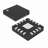
MAX4206ETE+T Maxim Integrated Products, MAX4206ETE+T Datasheet - Page 9

MAX4206ETE+T
Manufacturer Part Number
MAX4206ETE+T
Description
IC AMP TRANS LOG 16-TQFN
Manufacturer
Maxim Integrated Products
Datasheet
1.MAX4206ETET.pdf
(17 pages)
Specifications of MAX4206ETE+T
Amplifier Type
Logarithmic
Number Of Circuits
1
Slew Rate
12 V/µs
Gain Bandwidth Product
5MHz
Voltage - Input Offset
1000µV
Current - Supply
5mA
Current - Output / Channel
58mA
Voltage - Supply, Single/dual (±)
2.7 V ~ 11 V, ±2.7 V ~ 5.5 V
Operating Temperature
-40°C ~ 85°C
Mounting Type
Surface Mount
Package / Case
16-TQFN Exposed Pad
Number Of Channels
1
Input Offset Voltage
5 mV
Operating Supply Voltage
3 V, 5 V, 9 V
Supply Current
5 mA
Operating Temperature Range
+ 85 C
Mounting Style
SMD/SMT
Power Dissipation
1349 mW
Lead Free Status / RoHS Status
Lead free / RoHS Compliant
Output Type
-
-3db Bandwidth
-
Current - Input Bias
-
Lead Free Status / Rohs Status
Details
(V
T
Amplifier with Over 5 Decades of Dynamic Range
A
CC
= +25°C, unless otherwise noted.)
-10
-20
-30
-40
-50
-60
10
0
PIN
1, 9
= +5V, V
10
11
12
13
14
15
16
2
3
4
5
6
7
8
100
C
R
COMP
COMP
SMALL-SIGNAL AC RESPONSE
1k
= 33pF
= 330Ω
EE
REFVOUT
CMVOUT
REFIOUT
REFISET
I
LOGIIN
= GND = 0V, I
LOGV1
OSADJ
LOGV2
LOG
FREQUENCY (Hz)
SCALE
REFIIN
CMVIN
NAME
GND
N.C.
10k
V
V
I
_______________________________________________________________________________________
LOG
CC
EE
TO V
= 1mA
I
I
LOG
I
LOG
LOG
LOGV1
100k
I
LOG
= 10µA
= 100µA
Precision Transimpedance Logarithmic
= 1µA
= 100nA
No Connection. Not internally connected.
1.238V Reference Voltage Output. Bypass REFVOUT to GND with a 0 to 1µF capacitor (optional).
Ground
Negative Power Supply. Bypass V
Logarithmic Amplifier Voltage Output 1. The output scale factor of LOGV1 is 0.25V/decade.
Offset Adjust Input. When operating from a single power supply, current applied to OSADJ adjusts
the output offset voltage (see the Output Offset section).
Scale Factor Input. Adjust the output scale factor for LOGV2 using a resistive divider (see the Scale
Factor section).
Logarithmic Amplifier Voltage Output 2. Adjust the output scale factor for LOGV2 using a resistive
divider (see the Scale Factor section).
Positive Power Supply. Bypass V
Current Reference Adjust Input. A resistor (R
REFIOUT (see the Adjusting the Logarithmic Intercept section).
0.5V Common-Mode Voltage Reference Output. Bypass CMVOUT to GND with a 0.1µF capacitor.
Current Reference Output. The internal current reference output is available at REFIOUT.
Current Reference Input. Apply an external reference current at REFIIN. I
current used by the logarithmic amplifier when generating LOGV1.
Current Input to Logarithmic Amplifier. LOGIIN is typically connected to a photodiode anode or other
external current source.
Common-Mode Voltage Input. V
amplifiers (see the Common Mode section).
1M
REF
= 1µA, I
10M
LOG
-10
-20
-30
-40
-50
-60
Typical Operating Characteristics (continued)
10
0
= 10µA, LOGV2 = SCALE, LOGV1 = OSADJ, CMVIN = CMVOUT, R
100
C
R
COMP
COMP
SMALL-SIGNAL AC RESPONSE
= 1kΩ
= 100pF
1k
I
LOG
CMVIN
I
CC
LOG
FREQUENCY (Hz)
EE
I
10k
LOG
= 100µA
I
LOG
TO V
to GND with a 0.1µF capacitor.
to GND with a 0.1µF capacitor.
= 10µA
I
= 1µA
LOG
is the common-mode voltage for the input and reference
LOGV1
100k
= 100nA
SET
FUNCTION
I
LOG
1M
), from REFISET to GND, adjusts the current at
= 1mA
10M
-12
-3
-6
-9
3
0
10k
SMALL-SIGNAL AC RESPONSE
100k
REFIIN
A
Pin Description
A
V
V
FREQUENCY (Hz)
= 2V/V
OF BUFFER
= 4V/V
is the reference
1M
10M
A
V
SET
= 1V/V
> 1MΩ,
100M
9


