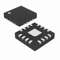
MAX4207ETE+T Maxim Integrated Products, MAX4207ETE+T Datasheet - Page 11

MAX4207ETE+T
Manufacturer Part Number
MAX4207ETE+T
Description
IC AMP TRANS LOG 16-TQFN
Manufacturer
Maxim Integrated Products
Datasheet
1.MAX4207ETET.pdf
(15 pages)
Specifications of MAX4207ETE+T
Amplifier Type
Logarithmic
Number Of Circuits
1
Slew Rate
12 V/µs
Gain Bandwidth Product
5MHz
-3db Bandwidth
1MHz
Current - Input Bias
10pA
Voltage - Input Offset
600µV
Current - Supply
5mA
Current - Output / Channel
58mA
Voltage - Supply, Single/dual (±)
2.7 V ~ 11 V, ±2.7 V ~ 5.5 V
Operating Temperature
-40°C ~ 85°C
Mounting Type
Surface Mount
Package / Case
16-TQFN Exposed Pad
Number Of Channels
1
Input Offset Voltage
2 mV
Supply Current
6 mA
Operating Temperature Range
+ 85 C
Mounting Style
SMD/SMT
Power Dissipation
1349 mW
Lead Free Status / RoHS Status
Lead free / RoHS Compliant
Output Type
-
Lead Free Status / Rohs Status
Details
Substituting into the TE approximation,
As a worst case, one finds TE ≅ ±178mV or ±3.6% of
full scale.
When expressed as a voltage, TE increases in proportion
with an increase in gain as the contributing errors are
defined at a specific gain. Calibration using a look-up
table eliminates the effects of gain and output offset
errors, leaving conformity error as the only factor
contributing to total error. For further accuracy, consider
temperature monitoring as part of the calibration process.
Five decades of input current across a 10nA to 1mA
range are acceptable for I
bias currents increase as I
10nA. Bandwidth decreases at low I
the Frequency Response and Noise Considerations
section). As I
transistors become less logarithmic in nature. The
MAX4207 incorporates leakage current compensation
and high-current correction circuits to compensate for
these errors.
The MAX4207’s frequency response is a function of the
input current magnitude and the selected compensation
network at LOGIIN and REFIIN. The compensation net-
work comprised of C
over the specified range of input currents by introducing
an additional pole/zero to the system. For the typical
application, select C
The MAX4207 bandwidth is proportional to the magnitude
of the I
inversely proportional to I
A 0V common-mode input voltage, V
able at CMVOUT and can be used to bias the logging
and reference amplifier inputs by connecting CMVOUT
to CMVIN. A voltage between 0 and 0.5V, connected to
CMVIN, may be used to bias the logging and reference
transistor collectors, thereby optimizing performance.
Amplifier with Over 5 Decades of Dynamic Range
TE ≅ ± (1V/decade)(0.05 log
Frequency Response and Noise Considerations
REF
±4 (±5mV ±2mV) = ±[0.15V ±4(±7mV)]
and I
LOG
Applications Information
LOG
______________________________________________________________________________________
and I
COMP
COMP
Frequency Compensation
currents, whereas the noise is
REF
REF
Precision Transimpedance Logarithmic
= 32pF and R
LOG
and R
increase to 1mA or higher,
and I
Input Current Range
LOG
and I
LOG
10
COMP
and I
(100µA/100nA)
Common Mode
REF
currents.
CMVOUT
LOG
ensures stability
COMP
. The effects of
REF
values (see
fall below
= 330Ω.
, is avail-
Adjust the logarithmic intercept by changing the refer-
ence current, I
(see Figure 5) adjusts the reference current, according
to the following equation:
where V
5MΩ. REFIOUT current range is 10nA to 10µA only.
The MAX4207 operates only from dual ±2.7 to ±5.5V sup-
plies. The relationship of inputs to outputs is a function of
I
mitted amplifier. The uncommitted amplifier can be con-
figured in either inverting or noninverting mode. In an
inverting configuration, the uncommitted amplifier output,
LOGV2, is positive and LOGV1 is negative when I
exceeds I
ration, LOGV2 and LOGV1 are both negative when I
exceeds I
the uncommitted buffer is recommended when large out-
put offset voltage adjustments are required using OSADJ.
By connecting CMVOUT and CMVIN, the log and refer-
ence amplifier inputs (LOGIIN and REFIIN) are biased at
0V. Applying the external voltage (0 to 0.5V) to CMVIN
optimizes the application’s performance.
Figure 5. Typical Operating Circuit
REF
, relative to I
I
IN
REFISET
R
330Ω
C
32pF
Adjusting the Logarithmic Intercept
COMP
REF
REF
COMP
0.1µF
C
. When operating in a noninverting configu-
R
COMP
(see Table 1). An inverting configuration of
32pF
50kΩ
330Ω
COMP
R
SET
REF
LOG
is 0.5V. Select R
R
SET
. A resistor from REFISET to GND
, and the configuration of the uncom-
=
LOGIIN
REFIOUT
REFIIN
CMVIN
CMVOUT
REFISET
V
10
REFISET
Dual-Supply Operation
×
MAX4207
I
REF
GND
V
V
CC
CC
SET
REFVOUT
V
V
between 5kΩ and
EE
EE
LOGV2
SCALE
LOGV1
OSADJ
0.1µF
V
OUT
R1
10kΩ
R4
R2
4kΩ
R3
LOG
LOG
11


