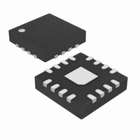
MAX4207ETE+T Maxim Integrated Products, MAX4207ETE+T Datasheet - Page 2

MAX4207ETE+T
Manufacturer Part Number
MAX4207ETE+T
Description
IC AMP TRANS LOG 16-TQFN
Manufacturer
Maxim Integrated Products
Datasheet
1.MAX4207ETET.pdf
(15 pages)
Specifications of MAX4207ETE+T
Amplifier Type
Logarithmic
Number Of Circuits
1
Slew Rate
12 V/µs
Gain Bandwidth Product
5MHz
-3db Bandwidth
1MHz
Current - Input Bias
10pA
Voltage - Input Offset
600µV
Current - Supply
5mA
Current - Output / Channel
58mA
Voltage - Supply, Single/dual (±)
2.7 V ~ 11 V, ±2.7 V ~ 5.5 V
Operating Temperature
-40°C ~ 85°C
Mounting Type
Surface Mount
Package / Case
16-TQFN Exposed Pad
Number Of Channels
1
Input Offset Voltage
2 mV
Supply Current
6 mA
Operating Temperature Range
+ 85 C
Mounting Style
SMD/SMT
Power Dissipation
1349 mW
Lead Free Status / RoHS Status
Lead free / RoHS Compliant
Output Type
-
Lead Free Status / Rohs Status
Details
ABSOLUTE MAXIMUM RATINGS
(All voltages referenced to GND, unless otherwise noted.)
V
V
Supply Voltage (V
REFVOUT ....................................................(V
OSADJ, SCALE, REFISET ...........................(V
REFIIN, LOGIIN ........................................(V
LOGV1, LOGV2, CMVOUT,
CMVIN............................................................(V
Precision Transimpedance Logarithmic
Amplifier with Over 5 Decades of Dynamic Range
Stresses beyond those listed under “Absolute Maximum Ratings” may cause permanent damage to the device. These are stress ratings only, and functional
operation of the device at these or any other conditions beyond those indicated in the operational sections of the specifications is not implied. Exposure to
absolute maximum rating conditions for extended periods may affect device reliability.
DC ELECTRICAL CHARACTERISTICS—Dual-Supply Operation
(V
T
2
CC
EE
A
Supply Voltage
Supply Current
LOGIIN Current Range
(Notes 3, 4)
REFIIN Current Range
(Notes 3, 4)
Common-Mode Voltage
Common-Mode Voltage Input
Range
Log Conformity Error
Logarithmic Slope (Scale Factor)
Logarithmic Slope (Scale Factor)
Temperature Drift
Input Offset Voltage
Input Offset Voltage Temperature
Drift
Voltage Reference Output
CC
REFIOUT ......................................(V
= -40°C to +85°C. Typical values are at T
............................................................................-6V to +0.3V
...........................................................................-0.3V to +6V
_______________________________________________________________________________________
= +5V, V
PARAMETER
EE
CC
= -5V, GND = 0, I
to V
EE
) .............................................. +12V
REF
V
SYMBOL
V
EE
V
REFVOUT
CMVOUT
= 1µA, I
I
CMVIN
V
V
I
V
V
- 0.3V) to (V
I
LOG
V
REF
CC
IOS
CC
K
EE
LC
IO
EE
A
EE
EE
- 0.3V) to V
= +25°C, unless otherwise noted.) (Note 1)
EE
- 0.3V) to +3.0V
- 0.3V) to +5.5V
LOG
- 0.3V) to +1V
(Note 2)
(Note 2)
T
T
Minimum
Maximum
Minimum
Maximum
I
I
K = -0.25V/decade
(Note 4)
T
T
T
T
|V
|V
T
T
REF
LOG
A
A
A
A
A
A
A
A
CMVIN
CMVIN
CC
= 10µA, LOGV2 = SCALE, LOGV1 = OSADJ, CMVIN = CMVOUT, R
= +25°C
= +25°C
= +25°C, |V
= +25°C
= -40°C to +85°C
= -40°C to +85°C
= -40°C to +85°C
= -40°C to +85°C (Note 4)
= 10nA to 1mA,
= 10nA,
+ 0.3V)
CMVIN
- V
- V
LOGIIN
REFIIN
CMVIN
CONDITIONS
|, |V
|
Continuous Current (REFIIN, LOGIIN) ................................10mA
Continuous Power Dissipation (T
Operating Temperature Range ...........................-40°C to +85°C
Junction Temperature .....................................................+150°C
Storage Temperature Range .............................-65°C to +150°C
Lead Temperature (soldering, 10s) .................................+300°C
16-Pin Thin QFN (derate 16.9mW/°C above +70°C) ...1349mW
CMVIN
- V
T
T
REFIIN
A
A
= +25°C
= -40°C to +85°C
- V
|,
LOGIIN
|
-231.25
-237.5
1.218
1.195
MIN
-2.7
2.7
10
10
0
A
= +70°C)
1.238
-250
TYP
0.6
±2
80
5
0
6
- 268.75
-262.5
1.258
1.275
MAX
±10
-5.5
5.5
7.5
0.5
±5
6
1
1
5
SET
decade/
decade
UNITS
> 1MΩ,
µV/°C
mV/
mA
mA
mA
mV
µV/
mV
nA
nA
°C
V
V
V
V


