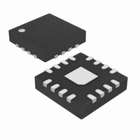
MAX4206ETE+ Maxim Integrated Products, MAX4206ETE+ Datasheet - Page 11

MAX4206ETE+
Manufacturer Part Number
MAX4206ETE+
Description
IC AMP TRANS LOG 16-TQFN
Manufacturer
Maxim Integrated Products
Datasheet
1.MAX4206ETET.pdf
(17 pages)
Specifications of MAX4206ETE+
Amplifier Type
Logarithmic
Number Of Circuits
1
Slew Rate
12 V/µs
Gain Bandwidth Product
5MHz
Voltage - Input Offset
1000µV
Current - Supply
5mA
Current - Output / Channel
58mA
Voltage - Supply, Single/dual (±)
2.7 V ~ 11 V, ±2.7 V ~ 5.5 V
Operating Temperature
-40°C ~ 85°C
Mounting Type
Surface Mount
Package / Case
16-TQFN Exposed Pad
Number Of Channels
1
Input Offset Voltage
5 mV
Operating Supply Voltage
3 V, 5 V, 9 V
Supply Current
5 mA
Operating Temperature Range
+ 85 C
Mounting Style
SMD/SMT
Power Dissipation
1349 mW
Lead Free Status / RoHS Status
Lead free / RoHS Compliant
Output Type
-
-3db Bandwidth
-
Current - Input Bias
-
Lead Free Status / Rohs Status
Details
where:
K = scale factor (V/decade)
I
I
The MAX4206 uses internal temperature compensation
to virtually eliminate the effects of the thermal voltage,
(kT/q), on the amplifier’s scale factor, maintaining a
constant slope over temperature.
The ideal logarithmic amplifier transfer function is:
Adjust K (see the Scale Factor section) to increase the
transfer-function slope as illustrated in Figure 3. Adjust
I
Intercept section) to shift the logarithmic intercept to the
left or right as illustrated in Figure 4.
Log conformity is the maximum deviation of the
MAX4206’s output from the best-fit straight line of the
V
a percent of the full-scale output or an output voltage.
Figure 2. Simplified Model of a Logarithmic Amplifier
LOG
REF
REF
Amplifier with Over 5 Decades of Dynamic Range
LOGV1
= the reference current at REFIIN
using REFISET (see the Adjusting the Logarithmic
= the input current at LOGIIN
LOGIIN
CMVIN
REFIIN
versus log (I
I
I
REF
LOG
V
IDEAL
______________________________________________________________________________________
LOG
=
K
Precision Transimpedance Logarithmic
/I
×
V
V
V
V
REF
CC
CC
EE
EE
log
) curve. It is expressed as
10
I
I
LOG
REF
Transfer Function
Log Conformity
Definitions
V
V
BE1
BE2
The log nature of the MAX4206 insures that any addi-
tive error at LOGV1 corresponds to multiplicative error
at the input, regardless of input level.
Total error (TE) is defined as the deviation of the output
voltage, V
the Transfer Function section):
Total error is a combination of the associated gain,
input offset current, input bias current, output offset
voltage, and transfer characteristic nonlinearity (log
conformity) errors:
where V
put offset voltages, respectively. Output offset is
defined as the offset occurring at the output of the
MAX4206 when equal currents are presented to I
and I
a gain of K = 0.25V/decade, a 4 should multiply the
(±V
from this default configuration.
Figure 3. Ideal Transfer Function with Varying K
V
LOGV
LC
Referred-to-Input and Referred-to-Output Errors
REF
±V
2
LC
=
. Because the MAX4206 is configured with
OSOUT
LOGV1
K
and V
-3
-1
-2
-4
(
3
4
2
1
0
1
0.001
±
∆
V
K
OUT
) term, if V
, from the ideal transfer function (see
V
OSOUT
) log
LOGV
IDEAL TRANSFER FUNCTION
= K LOG (I
CURRENT RATIO (I
10
WITH VARYING K
0.1
1
I
I
are the log conformity and out-
LOG
LOG
REF
=
LC
V
/I
IDEAL
REF
−
−
and V
)
I
I
BIAS
BIAS
K = 1
K = 0.5
K = 0.25
LOG
10
±
2
1
/I
±
OSOUT
REF
TE
)
4
(
±
V
LC
were derived
1000
Total Error
±
V
OSOUT
LOG
)
11


